Leave a comment

Classification basis of PCB design engineers

PCB design engineers have grading basis: introduction, elementary, intermediate (ABC), and advanced.Let’s have a look at what level of yourself.

Jobs: entry-level PCB engineers

Capacity requirements:

1, to create a simple package, such as DIP10 ;

2, to master the basic operation of at least one PCB design software, and can develop simple wiring width and spacing ;

3, to make reasonable and orderly layout and routing for the PCB with 100 components and 200 network or less.

4, to do the routing manually or automatically under the rules made by others or yourself and modity the routing,and 100% completion and DRC is completely passed.

5, to have the knowledge of the basic mechanical structure and thermal design

6, to have some basic requirements for double-sided traces.

Work:

1, design and modification of simple PCB,such as simple structure of the front panel,small single chip system board, etc.

2, specified part lines in complex PCB

3, the related debugging of their own pcb design.

4, write related development and debug logs.

Job duties: responsible for the part designed by yourself in the PCB.

Jobs: primary PCB engineers

Capacity requirements:

1, according to the manual and physical ,produce more complex packages such as lighted RJ-45 seat and so on, and to ensure that the size of shape and PAD is entirely correct (according to physical measurements ,to ensure that at least it can be inserted);

2, a master of at least one PCB design software,and can make detailed routing rules independently or under the guidance of others.

3, make reasonable and orderly layout and routing for the single-sided,double-sided and multilayer PCB with 400 components and 1000 network or less.During the layout and routing,consider the requirement of thermal design, structural design, electromagnetic compatibility design, aesthetics in a timely manner.When he is not sure,he should ask the more advanced PCB engineers for help or discuss with them.

4, expertly do the routing manually or automatically under the rules made by others or yourself and modity the routing,and 100% completion and DRC is completely passed.Basically there is no bottleneck of line width and the inner islands and other issues.During the routing ,he can find the stupid mistake on the principle of design and put forward the mistakes,and can correctly swap the pin and gate,and can correctly modify netlist and schematic.

5, correctly import and export mechanical drawings and basically understand structure size requirements;

6, He can proceed some high-speed and simulation PCB design under the rules or the guidance setted by others and basically stable

7, silk screen is clear.Independently complete design output work,such as Gerber, and proofread.

8, have a basic manufacturability aspects knowledge and use it for practice.More than 50% designed board can be used for production.

Work:
1, more complex PCB design and modification (eg scheduler boards in addition to CPU board , etc.);

2, specified part lines in complex PCB

3, the related debugging of their own pcb design.

4, for the work guidance of all lower-level PCB engineer;

5, write related development and debug logs.

6,if necessary,(that is to say you temporarily have no design task at a certain time,or some PCB design time is pressing,and we must transfer or strengthen the designer) you do the work of any low-level PCB engineer .

Job duties: responsible for the part designed by yourself in the PCB.

Jobs: intermediate PCB engineers (according to individual ability,it is subdivided into A, B, C three gears. A is supreme and B is the second)

Capacity requirements:
1, fully understand the various original components manuals and wiring manuals.Independently produce extremely complex packages such as placing the switch, and ensure that the capabilities entirely correct (according to physical measurements, ensure that at least the insertion).According to the principles and structural requirements on their own, find the right device or replacement

2,a skillful master of operation and skills of at least one PCB design software,and can make detailed routing rules .

3, put forward division and integration idea of various functional blocks according to the system requirements. Make reasonable layout and routing for any PCB with many components and network independently or cooperatively.During the layout and routing,consider the requirement of thermal design, structural design, SI,PI,EMC,aesthetics,and manufacturability in a timely manner and propose solutions.Can provide requirements and rules of some layout and wiring for entry-level and junior engineers.

4, correctly do the lamination design for PCB.Under the requirement that satisfy the performance ,try to minimize the number of layer and reduce the cost.

5, with more high-speed PCB design and simulation knowledge in the aspect of resistance, delay, overshoot, crosstalk, circuit, signal circuit, surface integrity, the inner slot, signal termination.Independently or under the guidance of SI engineers,complete SI simulation and analysis of key signal and regional and provide the improvement suggest.

6, under rule driven,skillfully rout by manual or automatic and pass the modification.The whole plate has a certain beauty.During the routing ,he can find the stupid mistake of 80% on the principle of design and put forward the mistakes,and can correctly swap the pin and gate.

7, He can be an excellent communication with the principles and structural design engineers. He can understand more complex mechanical drawings.He can put forward some reasonal improvement suggest of some principles,component selection ,and structure related PCB,and help system design early success.

8,test points and silk screen marking are clear and error-free.He makes few stupid mistakes in PCB design.Generally not due to PCB design error which led to the revision.The feedback,provide by more than 90% pcb factory engineers, can be always resolved by himself.

9, with more manufacturability aspects knowledge and use it for practice.More than 70% designed board can be used for production.

Work:
1, very complex PCB designs and modifications (such as 8-channel DVR chassis, PC motherboards, etc.);

2, the related debugging of their own pcb design.the SI simulation of specified position.

3, for the work guidance and routing rules of all lower-level PCB engineer;

4, write related development and debug logs.

5, production and maintenance for unit internal PCB standard package libraries and standard wiring module;

6, if necessary, do the work of any low-level PCB engineer .

Responsibilities:
1,responsible for the part designed by yourself in the PCB.

2,responsible for the part designed by yourself in unit internal PCB standard package libraries and standard wiring module.

3,responsible for their own SI simulation results and solutions.

Jobs: Senior PCB Engineer

Capacity requirements:
1, a master of document conversion between variety of common pcb design software.The document can be used to modify basically.

2, familiar with all the requirements of high-speed and simulation PCB design.More than 80% boards, designed by himself or by others but under his instruciton ,have no related issues.

3, with skillful manufacturability aspects knowledge and use it for practice and gudance work.More than 90% boards ,designed by himself or by others but under his instruciton ,can be used for mass production derictly.

4,skillful for high-density layout and routing under the high-speed rules.The module or board should be stable and reliable,and the same time,more than 80% board have great beauty.

5, very innovative, can often make various constructive proposals to improve PCB design efficiency, PCB design quality, PCB structure allocation in system.

Work:
1, to participate analysis, planning and simulation related to PCB in system design.

2, organize and carry out PCB design training;

3,for the work guidance and routing rules of all lower-level PCB engineer;

4, write related development and debug logs.

5,search, establishment, and file of SI simulation model.

6, SI, PI, EMC simulation of the entire board and system.Evaluation of PCB manufacturability . Analysis of defective PCB, and provide the effectibe solutions.

7, if necessary, do the work of any low-level PCB engineer.

Responsibilities:
1, responsible for all of their work;

2, responsible for guidance work of all the others.

Leave a comment

Are you sure you thoroughly understand the PCB design yet?

First: preparation. This includes preparing component libraries and schematics. “To do a good job, one must first sharpen one’s tools”.To make a good board, in addition to good PCB design principles,drawing should also be well. Before PCB design,firstly component library of SCH schematic and PCB should be ready.Component library can use protel own libraries, but under normal circumstances it is difficult to find a suitable one.It is better to do the component library yourself according to the standard size data of the selected device. In principle, do first PCB component library, then do SCH component library. Requirements of PCB component library are higher,which directly affects the board installation.SCH component library requires relatively loose.As long as the attention to pin attributes and corresponding relationship with the PCB components. PS: Note hidden pins in the standard library. After that it is the schematic design.After finishing the schematic design,it is ready to do PCB design.

Second: PCB design. This step draws PCB board in the PCB design environment according to determined board size and the mechanical positioning,and according to the positioning requirements put the connector, button or switch, screw holes, mounting holes and so on. And fully consider and determine the wiring area and the non-wiring area .For example, how much area around the screw holes belongs to the non-wiring area?

Third: PCB layout. Layout means to put the device on the board. Then if the preparations mentioned above are ready, then you can generate a netlist (Design-> Create Netlist) on the schematic, and then import the netlist (Design-> Load Nets) on the PCB drawing.The components are all put up.There are fly line prompt connection among the pins.Then you can make layout for the device.

The following principles of the general layout :
①. According to the electrical performance,do the reasonable zoning,which generally can be divided into: digital circuit area where is fear of interference, and also makes interference, analog circuit area where is fear of interference,power driver region where is interference source;
②. When performing the same function circuit,they should be placed as close as possible, and we should adjust various components to ensure the connection is the most simple; At the same time, adjust the relative position of each block to make sure the connection among the function block is the most simple;
③. For large mass components, the installation location and mounting strength should be considered. The heating elements should be placed separately from the temperature-sensitive components.When necessary, thermal convection measures should be considered.
④. I / O driver device should be as close to the edge of the printing plate as possible,and near the lead connector;
⑤. A clock generator (eg: Crystal or Restructure) tries to close the device which may use this clock ;
⑥. Between power input pin and ground in each IC, you need to add a decoupling capacitor (generally monolithic capacitors with good high-frequency performance are used.) when board space is more dense, you can also add tantalum capacitors around a few integrated circuits.
⑦.The place of relay coil should be added the discharge diode (1N4148 is OK).
⑧. Layout requirements should be balanced and orderly. The layout can not be biased towards one end.

– Pay special attention:when placing components,the actual size (occupied area and height) of components and the relative position between the components must be considerred,in order to ensure the electrical performance of the circuit board and the feasibility and convenience of production and installation. At the same time,on the premise of guarantee to reflect the above principles ,appropriate modification of device placement makes it neat and beautiful.For example, the same device should be placed neatly in the same direction,and can not be put too “patchwork.” This step is related to the overall image of the board and the degree of difficulty in the next wiring.So it takes great effort to consider.When making the layout,you can make the preliminary wiring for the place where you are not sure.And you should have full consideration.

Fourth: cabling. Cabling is the most important step in entire PCB design.This will directly affect the performance of PCB is good or bad .In the PCB design process, the wiring is generally divided three realms: first,the wiring is smooth,which is the basic requirement of PCB design. If the line is not smooth, and everywhere is the fly line,that would be defective board. Followed by the meet of the electrical performance,which is a standard that can be used to measure the board is qualified or not.After the wiring is smooth, carefully adjust the wiring so that it can achieve the best electrical performance. Next it is beautiful.If your wiring is smooth,and there is no place which can effect electrical properties,but all is in a mess,even if electrical performance is good, in others’ eyes,it is just a piece of garbage,which cause great inconvenience for the test and maintenance.Wiring should be uniform,not maintenance.These can be achieved under the condition than can ensure the electrical properties and meet other individual requirements, or you concentrate on the trifles and neglect the essentials.

When wiring mainly according to the following principles:
①. Under normal circumstances,firstly do the wiring of power and ground wiring to ensure the electrical performance of the circuit board.Within the range of allowing conditions ,try to widen the power and ground line.It is better that ground line is wider than power line.Their width relationship is :Ground lines > power lines > signal lines. Generally signal line width is 0.2 ~ 0.3mm , the smallest width is up to 0.05 ~ 0.07mm,and the power lines is usually 1.2 ~ 2.5mm.For the PCB of digital circuit, you can use wide ground wire to form a loop,and that become a ground network to use(analog circuits can not be usde like this)
②.Do the wiring in advance for lines with the more stringent requirements,such as high frequency line.The edges of input and output terminal should avoid adjacent parallel,in order to avoide reflection interference.If necessary, add ground line to isolation.The wiring in two adjacent layers should be vertical.If they are paralles, it is to cause parasitic coupling.
③. Chassis of oscillator is on ground.The clock line should be as short as possible,and can not be attracted everywhere.
④. Do the wiring with 45° polyline as far as possible.Do not use 90° polyline,which reduce radiation of high frequency signal
⑤. Any signal lines do not form a loop.If it is inevitable, the loop should be as small as possible; via of signal lines should be as little as possible;
⑥. The key line should be short and thick, and is surrounded with protective ground.
⑦. When transmitting sensitive signal and the noise field signal through the flat cable, use the way of “Ground – Signal – ground” to leads.
⑧. Test points should be set aside for the key signal, to be convenient for the production and maintenance .
⑨. After completion of schematics wiring, wiring should be optimized.

– PCB wiring process requirement

①Line
In general, width of the signal line is 0.3mm (12mil), and the power line width is 0.77mm (30mil) or 1.27mm (50mil); the distance between lines and the distance between the lines and the pad are not less than 0.33mm (13mil ).In the actual application, if conditions permit, increasing the distance should be considered.When wiring density is higher,using two lines between IC feet can be considered,but not recommended.Line width is 0.254mm(10mil),and line spacing is not less than 0.254mm (10mil). In special cases, when the device pin is dense, the line width and line spacing can be appropriately reduced.

②. Pad (PAD)
The basic requirements of PAD and VIA are: diameter of PAD is larger 0.6mm than the hole . For example,for universal pin-type resistors, capacitors and integrated circuits,if the diameter of PAD is 1.6mm(32mil) and the diameter of holes is 0.8mm(32mil),the size of sockets, pins and diode 1N4007, etc should be 1.8mm (71mil)or 1.0mm(39mil).In practical application, the size of PAD should be based on the actual size of the element.Conditionally, it may be appropriate to increase the size of the pad;The diameter of element mounting holes in PCB should be larger 0.2 ~ 0.4mm than the actual size of the element tin.

③. Vias (VIA)
Typically it is 1.27mm (50mil ) or 0.7mm ( 28mil);
When witing density is high,the via size can be ruduced appropriately,but not too small.You can consider 1.0mm(40mil) or 0.6mm ( 24mil)

(4)Spacing requirements of pad, line, and hole
PAD and VIA : ≥ 0.3mm(12mil)
PAD and PAD : ≥ 0.3mm(12mil)
PAD and TRACK : ≥ 0.3mm(12mil)
TRACK and TRACK : ≥ 0.3mm(12mil)

When the density is higher:
PAD and VIA : ≥ 0.254mm(10mil)
PAD and PAD : ≥ 0.254mm(10mil)
PAD and TRACK : ≥ 0.254mm(10mil)
TRACK and TRACK : ≥ 0.254mm(10mil)

Fifth: wiring optimization and screen printing.
“There is no best, only better”! No matter how you rack their brains to design,after you finish the painting, and take a look, still feel a lot of places that you can modify. General design experience are: the time of wiring optimization is twice than the initial wiring time.If I feel no need to modify the place,you can shop the copper (Place-> polygon Plane).The shopped copper is generally ground wire(note that the analog ground shoulde separated from the digital ground).If multilayers. power may also be paved. For the silk screen,it can not be blocked by the device or removed by vias and pads . Meanwhile,when design,you should face the component layer,and the bottom layer should be mirrored, in order to avoid confusion level.

Sixth: The network and the DRC and structural inspection. First, under the circumstance of the right circuit schematic design,do the physical connection relationship check for the generated PCB network files and schematics network file.And timely correct the design according to the output file results, to ensure that the wiring connection relationship is right.After the network is checked and passed,check the pcb design by DRC.And timely correct the design according to the output file results, to ensure electrical performance.Finally, check and confirm the pcb mechanical mounting strcutre.

Seventh: making the board. Before that, it is better to have a review process.

PCB design is the work of a mind .People, whose mind is dense and experience is rich, design the board that is indeed good.So be extremely careful when design, and fully consider all aspects of the factors (for example, ease of maintenance and inspection that a lot of people do not consider).Be excelsior , we will be able to design a good board.

Leave a comment

The role of electrolytic capacitor in the circuit design

16053101_pcb
When talking about electrolytic capacitor, we shall know more about its role.

1, the filtering effect: in the power circuit, a rectifying circuit makes alternating current into the pulsating direct current.After a rectifier circuit ,access electrolytic capacitor of larger capacity.Using the properties of charge and discharge makes pulsating direct current voltage become relatively stable direct current voltage.

In practice, in order to prevent supply voltage of various parts of pcb manufacturing from change because of the change of electronic load, so the output of the power and the input of the power of the load generally have electrolytic capacitors of tens to hundreds of microfarads. Because large-capacity electrolytic capacitors generally have a certain inductance, which can not effectively filter out high frequency and pulse interference signal,so it has a capacitor with a capacity of 0.001–0.1 pF in parallel at both ends to filter out high frequency and pulse interference.

2, coupling effect: in transmission and amplification process of the low-frequency signal ,to prevent quiescent point of the front and back two level circuit from interaction effect,we often use the
capacitive coupling.To prevent too large loss of the low frequency component of the signal in the signal ,we usually use electrolytic capacitors with larger capacity.

Then we have to look at the judging method of electrolytic capacitors

Common faults of Electrolytic capacitor are : capacity reduce; the capacity disappear; breakdown ,short circuit and leakage.capacity change is caused by the gradual drying of the its inner electrolyte solution during the its use or place.While breakdown and leakage are caused by too high voltage that is added ro by itself poor quality.

Analyzing quality of the power capacitors of PCB prototype,we generally use the resistance of a multimeter to measure. Specific methods are: make two pins of capacitors short circuit ,to discharge,and then connect the positive of electrolytic capacitor with black pen of a multimeter ,connect the negative with red pen,which is for the pointer multimeter.If for digital multimeter,when measuring,the pens should have intermodulation. Normally hands should firstly swing in the direction of small resistance,then gradually return until infinity.If amplitude of swing of the hands is larger,or the return rate is slower,it indicates that the capacity of capacitor is greater.Otherwise, it indicates the capacity of capacitor is smaller.If the hand means no change somewhere in the middle,it indicates that this capacitor is leakage.If the resistance indicator value is very small or zero,it indicates that this capacitor is short-circuit breakdown.

Voltage of Battery that multimeter uses is generally low,so it is more accurate when measuring low-voltage capacitors, and when measuring high-voltage capacitor,although the measurement is normal,but when coupled with high pressure,it may appear leakage or breakway.

More attention to understanding the use of electrolytic capacitors

1, electrolytic capacitor has polarity, so the circuit can not be reversed . In the power supply circuit, when the output voltage is positive,then the positive of electrolytic capacitors connect the output of power,and the negative connect the ground.when the output voltage is negative,then the positive connect the output ,and the negative connect the ground.

When filter capacitor polarity of the power supply circuit reverse,because the filtering effect of the capacitor greatly reduce,which on the one hand cause fluctuation of power output voltage. On the other hand ,the reverse current makes electrolytic capacitors which is equivalent to resistance heat. When the reverse voltage exceeds a certain value, the reverse leakage resistance of capacitance will become very small,after power,it works soon,which can make the capacitor overheat, and then burst and damage.

2, voltage applied to both ends of the electrolytic capacitor can not exceed its allowable operating voltage. In the actual circuit design , a margin should leave depending on the circumstances.In the design of filter capacitor of stabilized voltage supply,if the voltage of AC power is 220v,secondary rectifier voltage of transformer can be up to 22v.When pcb prototype,using electrolytic capacitors of 25v can generally meet the requirements.

However, if fluctuations of the AC power supply voltage are large and likely to rise to more than 250V, it is better to use the electrolytic capacitor of 30V or more.

3, electrolytic capacitors in the circuit should not be close to the heating element with high power, to prevent electrolyte solution from accelerated drying because of the heat.

4, for the positive and negative polarity signal filtering ,we can use the method that two electrolytic capacitors connect in series with the same polarity,which can be treated as non-polar capacitor.

5, capacitor case, the auxiliary leads terminal, the positive and negative ,and the pcb board must be completely isolated.

Leave a comment

PCB reliability problems and case analysis

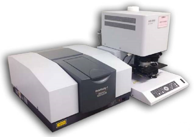
Infrared spectrometer

Fourier transform infrared spectroscopy (FTIR) use the Michelson interferometer to make two beams of coherent infrared light flash on the sample,collected by the detector,to obtain infrared interferogram data that contain sample information. After the computer transform date through Fourier, to abtain IR spectra of samples , to study molecular structure and chemical bonding of the detected substance though the IR spectra.

FTIR is widely used in the detection of organics .
16060801_pcb

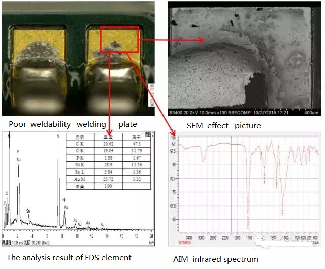
In PCB/PCBA failure analysis, it combines the attenuated total reflection (ATR) with infrared microscopy (AIM). It can have ualitative analysis of organics in pcb manufacturing process and PCB/PCBA surface organic foreign bodies.

ATR is easy to operate,and it has low requirements on sample preparation.It can detect solid and liquid organic without special treatment .It goes for analysis of large amount of organic of PCB/PCBA,but it is more difficult for small samples for testing.If ATR is used for the analysis of detecting degree of curing solder mask .The solder resist curing involves two processes: photo curing and heat curing,and they are the chemical reaction of propenyl group and an epoxy group in the ink ,respectively. FTIR Infrared spectra can detect the changes of functional groups before and after curing in ink ,to determine the curing situation of the solder resist.

16060802_pcb.webp

AIM compensate for the inadequacies of the ATR. For small sample, it has excellent detection performance,and it can detect the sample with the square less than 10μm * 10μm.At the same time, the amount of sample is required less.In theory, it can detect micron-level trace samples.In PCB \ PCBA failure analysis ,we usually use EDS to do compositional analysis of small amounts of substances,but EDS mainly analyze element content,and can not do the analysis for H.The analysis of organic is helpless.AIM ,as trace organics detection means,solve the problem of analyzing the pad surface trace organic. In the actual failure analysis,the joint use between AIM and EDS can do a comprehensive analysis of material composition.

16060803_pcb.webp

The infrared thermal imager

Infrared Thermal Camera is widely used to observe the surface temperature distribution.It can test the temperature distribution of objects under different conditions.Temperature monitoring range can reach 0-250 ℃,which has a wide range of testing.The sensitivity of testing the temperature is better than 100mK,which can clearly react the temperature distribution of the surface of the object in different regions.

16060804_pcb.webp

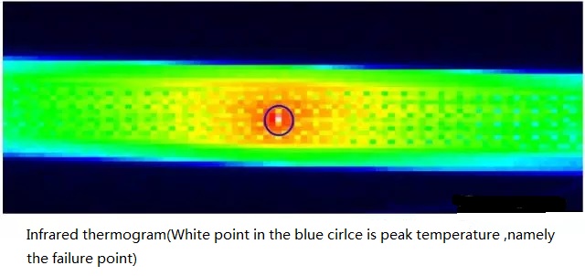
Infrared thermal camera use measured target’s infrared radiation energy distribution graphics,which are received by infrared detectors and optical imaging lens ,to reflect on the photosensitive element of infrared detectors,and thereby get the infrared thermography.This thermography is corresponds to the heat distribution field of the surface of objects.The different colours in the thermography represent different temperature of tested objects. Usually white is set to maximum temperature.

In PCB / PCBA failure analysis applications,infrared imaging ,as a means of non-destructive analysis, can locate complex networks ajar failpoints .The external current is applied to the PCB/PCBA failure network. Infrared camera observe the temperature distribution of PCB / PCBA surface.The failpoints will present the highest temperature point on the PCB/PCBA infrared thermogram,which can quickly locate ajar failpoints in complex network. This approach greatly improves the efficiency and accuracy of the failure analysis.

16060805_pcb.webp

X-Ray Inspection Machine

X-ray is the electromagnetic wave with short wavelength and great energy. Its photon energy is much larger tens of thousands to hundreds of thousands times than visible photon energy, with strong penetration .In physics, industry, agriculture and medicine ,as a means of non-destructive testing,it has been widely used.In the PCB manufacturing and mounting SMT industry,X-Ray detector is a commonly used testing equipment,and its minimum resolution can be up to 250nm,and it can observe the fine features.While its video receiver may have deflection angle of about 70 ° left and right (a total of 140 °) and rotate 360 °, which can achieve muli-directional observation at different angles.

16060806_pcb.webp

X-ray detection machine generate high-energy X-rays through the X-ray emitting tube,and make the high-energy X-ray irradiate to he test sample surface.Due to different density and atomic weight of sample material itself, the different components have different absorption capacity for the X-rays,and then generate projection on the image receiver.The higher density material has the deeper the shadow,and thus distinguish different material of samples.

In PCB / PCBA failure analysis applications,X-ray, as a means of non-destructive analysis, mainly is used in the analysis of solder joints, cracks, inner short circuit. Solder joints analysis are mainly used in the analysis of soler joints empty thta is generated in the process of SMT, as well as the analysis of cracks and short cut of the PCB circuit.And its analysis can analyze horizontal position and height of the defects by adjusting the viewing angle,and can perform the accurate location.

Leave a comment

The creative PCB designs absolutely stun your vision

When art and technology spark,it will let us shine, smile, or at least feel: Cool!

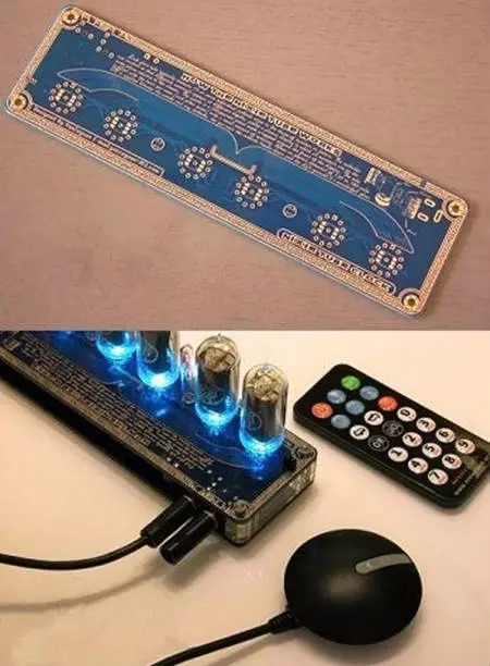
Classical style nixie tube clock

Yanzeyuan designed nixie tube clock . In addition to beautiful winding,the board also briefly describes the nixie tube clock and the principle that it works. The more common tube clock will be placed in a wooden or metal shell, and this works make the present of nixie tube clock have a totally different style.
16053002_pcb

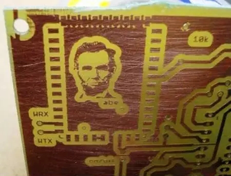
Make the idol’s face etched in PCB

Put the head image of the US President Abraham Lincoln into the circuit board design, perhaps it has his personal reasons, and perhaps just wiring with that function needs the drawing that is like the the head image of Lincon’s .But it’s really cool!
16053003_pcb

Skull Mini Synthesizer

The designer of this work is John Richards.It is another mini-synthesizer circuit board with a completely different style compared with above graffiti style.The skeletons in parallel row on the board is the keyboard of synthesizer .The space of oscillator is controlled by electrical level of skin contact. In fact, the secret of playing this little thing is that before you start playing, firstly lick your fingertips …
16053004_pcb

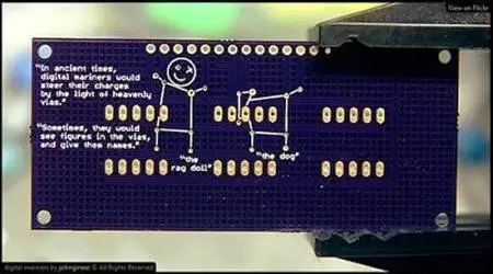
Join humor into circuit board design

Works are from johngineer designer. The through holes of the circuit board are like stars which can be imagined as different patterns!
16053005_pcb
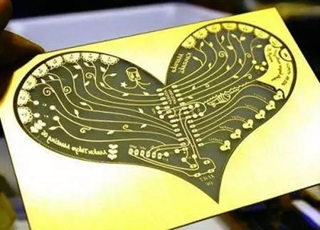
Arduino development board with love shape!

Your core circuit board can look like hearts!
16053006_pcb
A circuit board can become jewelry

This is a wearable circuit board design.It not only has a cool shape,but also can really become accessories.The circuit of this PCB can drive the light-emitting array of 16 LED,and it also can use the 12 mini solar battery on the board to charge.If you do not want to stand in the sun for too long, it can be charge with USB.It is very unique decoration!
16053007_pcb
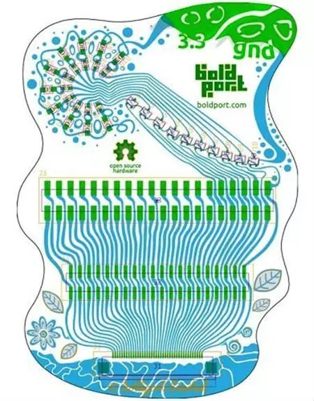
Design Beautiful board with software tools

The following circuit board design of audio plug adapter is drawn by PCBmodE software.Using the right tools,not only makes the function of your board complete,but also look more beautiful.
16053008_pcb
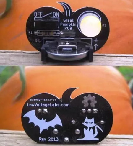
Pumpkin shape of PCB

This is a pumpkin PCB developed in low voltage labs. In addtion to the cute shape,it is also printed a lovely pattern. This board have LED bulbs.Even if you put it into the Halloween pumpkins lamp,you do not worry that the wind will blow out the candle. Even as decoration it also very nice!
16053009_pcb
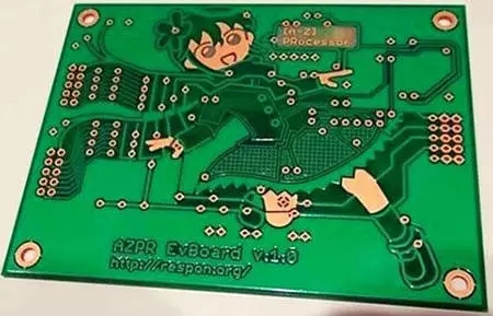
“Substrate girl” development Board with thick Japanese cartoon style.

Japanese engineer desighed the FPGA development board of Xilinx Spartan-3E series .Its spokesman ,who also has 3D three-dimensional doll ,has a very cute name called “substrate girl”;Its pattern on the board is not printed.It is composed of winding and ground plane. And otaku heart it?
16053010_pcb

Leave a comment

10 considerations of PCB panel

Share 10 considerations of PCB panel for fabrication:

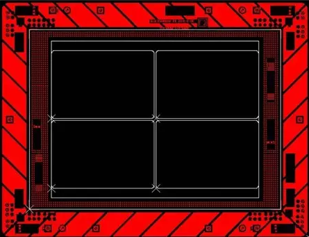
1, frame of PCB panel should use the design of closed loop,to ensure that PCB will not be deformed after fixing on fixture

2, the width of pcb panel ,for SIEMENS line, should be not more than 260mm ;for FUJI line, should be not more than 300mm.If it needs automatic dispensing,width *length should be not more than 125mm*180mm.

3, The shape of PCB panel try to close to square shape.We recommend using the panel of 2*2 and 3*3.

4, the center distance of the small board shoule be controlled between 75 mm and 145 mm.

5, When we set the base location point, usually leave solder-free zone where is more than 1.5mm than the base location point.

6, The junction ,between panel frame and inner small board,between small boards , does not have large components or protruding components.And the edge of components and pcb should have the space of more than 0.5mm,to ensure the normal operation of the cutting tool.

7, Make four positioning holes in the four corners of panel frame.The diameter is 4mm,and its tolerance is + 0.01mm. The strength of the hole should be moderate, to ensure that the holes can not be broken in the process of loading and unloading the board.Precision of aperture and position should be high.The hole wall should be smooth and burr-free.

8, Each small board in PCB panel should have at least three positioning holes,and its aperture is between 3mm and 6 mm. The place within 1mm of edge location does not allow wiring or patch;

9 Datum symbol is used for positioning of the entire board and fine-pitch devices .In principle,QFP with the space of less than 0.65mm should be set on diagonal position.The datum symbol should be used in pairs,and should be set on diagonal position of positioning elements.

10, Large components should have positioning column or positioning holes,such as I / O interface, microphone, battery connector, micro switch, headphone jack,and a motor.

Leave a comment

9 big advantages of using industrial robots instead of human in PCB manufacturing industry.

In recent years, China has gradually entered the aging society, the development of traditional labor-intensive enterprises is increasingly restricted.As a labor-intensive industry ,it’s more and more difficult for recruitment in PCB manufacturing industry . Applications of industrial robots have brought new impetus for the PCB industry.The fabrication mode that use the robots to operate the automation equipment, is gradually replacing the fabrication mode that human operate the automation equipment.What are the advantages that robots engaged in PCB manufacturing industry instead of human?
16060401_pcb.webp
1.Using robots can avoid potential threats that operating environment cause for workers’ health and safety,which save the investment in environmental security.

2. To enhance the accuracy of the job, improve product quality. Robot can use programming and vision system to achieve accurate positioning and repeat-ability,which effectively improve the quality of the product.

3.Effectively reduce material consumption rate.

4. To reduce labor, to expedite the work rhythm, to improve work efficiency. Robots can achieve higher-speed repetitive actions, can be much higher than the manual work rhythm,which lead to significantly enhancing the efficiency and reducing the costs of labor and management.

5.The robots can make the pcb manufacturing process flexibility. In future ,PCB industry will appear more and more small batches orders. Use of industrial robots can greatly improve production flexibility, to achieve rapid delivery of orders.

6. Reduce the state influence that cause by repetitive or boring process for workers .This state influence can lead to the decline of efficiency and quality.

7. Optimization of PCB manufacturing processes, reducing the space occupied by the production operations.

8. Continuous operation of 24 hours and work under black light environment;

9. To enhance the brand image and reputation. Applications of industrial robots make the level of automation of PCB manufacturers further enhanced,and can drive the progress of product quality, production efficiency, cost control, responsiveness, which improve the overall competitiveness of the manufacturers in the industry.

In fact, after conclusion,you can easily fint that the benefits that using industrial robote brings are mainly to improve the production efficiency,and to reduce some costs caused by hirer,and to improve product quality,and to provide the impetus for company competition.

Leave a comment

Production process control of miltilayer PCB

Due to the rapid development of high-tech, most electronic products are beginning to use multi-layered pcb. Traditional single and double-sided board can not meet requirements of the design and use. Multilayer PCB fabrication in the whole production has been dominant. For production process of multilayer boards,engineers in R & D job for many years have no chance to go to the pcb factory for understanding the entire production process control.

So, today,I will take the production process of our factory’s order 336058 as an example. From two aspects:the part of engineering design and the part of production process control, I will analysis the production process control of miltilayer pcb for everyone.

Product Overview – Production Difficulties
Layers is 10,
Minimum mechanical drilling is 0.2mm
L2 ~ L9 is for the buried hole, diameter is 0.2mm
L1 ~ L2 and L9 ~ L10 are for the blind hole, diameter of a blind hole is 0.127mm
Line width and line spacing are both 4mil
The thickness of inner core is 0.2mm,and its copper thickness is H / H oz

Engineering design part
Design of L2 ~ L9
16052801_pcb

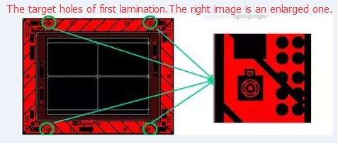
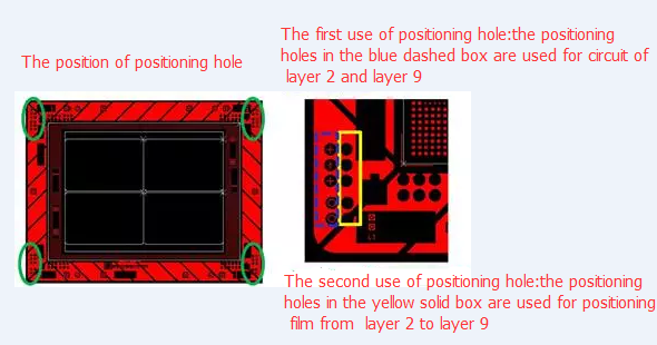
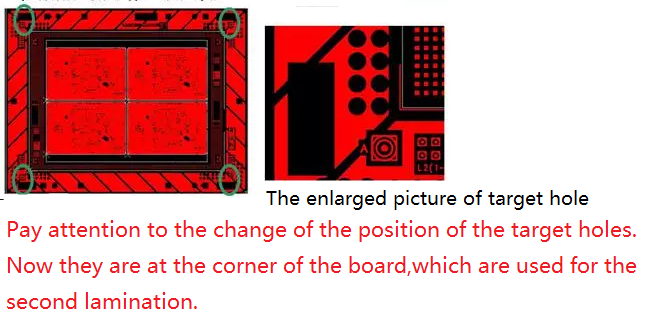
Lamination target hole design of L2 ~ L9
16052802_pcb

Positioning hole design of L2 ~ L9
16052803_pcb

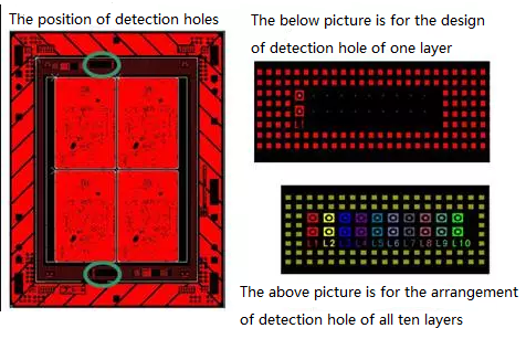
Detection hole design for buried hole of L2 ~ L9
16052804_pcb

Detection hole use for buried hole of L2 ~ L9
After finishing the lamination from layer 2 to layer 9,before drilliing the buried holes,we must drill the detection hole of buried hole.The size of detection hole and PAD is designed as the size of inner minimum hole.Therefore,when detection hole is detected with a magnifying glass by facing the light,if each layer are located in the PAD,it indicates that drilling the inner buried hole will not break pads.If the detection hole is outside PAD, it indicates that buried hole will deviate from the pad and appear open circuit.
16052805_pcb

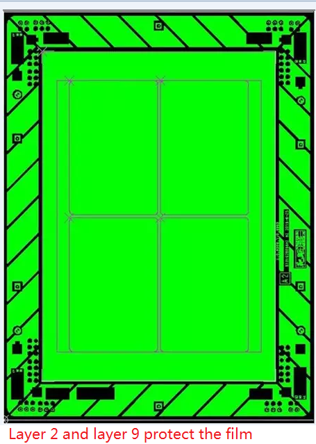
Layer 2 and layer 9 protect film
In the first time of inner layer line, layer 2 and layer 9 are not required to make the line, so when etching the inner layer , these two layers need to be protected with film.
16052806_pcb

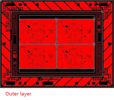
Making line of layer 2 and layer 9
16052807_pcb

16052808_pcb

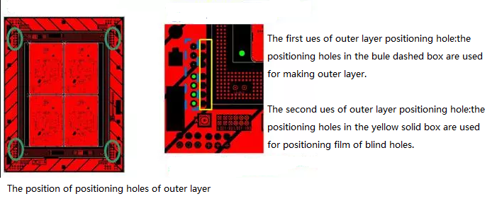
Use the outer positioning hole
16052809_pcb

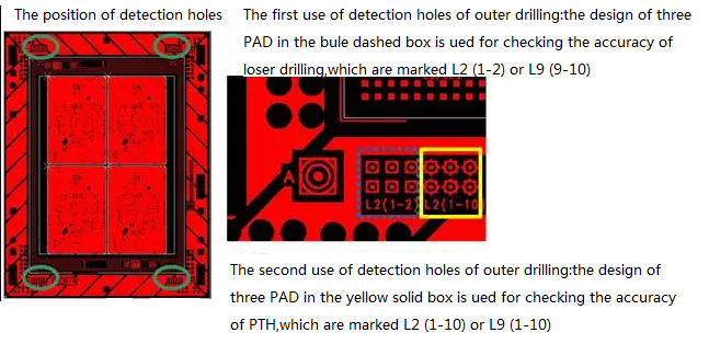
Detection hole of drilling hole (1)
16052810_pcb

Detection hole of drilling hole (2)
16052811_pcb

Use the detection hole of drilling hole
The design of these detection hole aims: When drilling, we can firstly drill detecion hole.If the drilled hole are within the range of detection PAD, it shows they are qualified,and the holes can be normally drilled.If the drilled hole are not within the range of detection PAD,it shows harmomegathus betweeen drill belt and board is inconsistent.At this time if the holes in the board are drilled,then mass open circuit will appear.At this time, you need to ask the project to adjust factor of harmomegathus.

NOTE: laser drilling will automatically adjust factor of harmomegathus according to the distance of four target holes.However, it requires that the target hole can not miss and that the bit between inner layers is not offset.

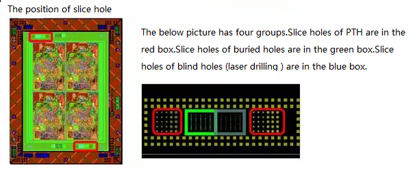
Slice hole
16052812_pcb
the content of engineering design part has been introduced over,and it is strictly controlled part when cam engineer deal with the production data. The next phase will continue for everyone about the” process control part “.

Leave a comment

Why you need fast turn PCB manufacturing services

When you have to satisfy requiring target dates and also pushing routines, fast turn PCB prototyping solutions are the very best options. Quick transform motherboard make sure that you have the ability to stay up to date with the following brand-new pattern out there, as well as do not drag the competitors. Merely mentioned, you require an extremely trusted company when you are trying to find fast turn preparations for your crucial tasks.

Quick transform jobs can either be turn-key or consigned, as well as you could pick the most effective choice in maintaining with the needs of your job. Commonly, leading PCB manufacturer will certainly provide you a selection of bundles depending upon the manufacturing amount, dimension of the PCB, kind of tooling and also wiring called for, and also the seriousness of your task.

Fast turn PCB companies could be gettinged on various forms of PCB such as round, rectangle-shaped, hexagonal, and so forth.

The finest component regarding a bundle method is that you do not require to throw away time figuring out the most appropriate remedy. Of training course, most PCB makers as well as developers likewise offer you the alternative of personalizing a specific bundle.

Right here are a few other needs to companion with a leading PCB production company:

Managing your PCB needs internal ask for substantial resources allowance as well as personnel financial investment. It could be a frustration because the existing financial circumstance where companies are coming to be leaner.

When you require a little manufacturing run, it is not practical to buy a whole selection of devices as well as tools. In such a situation, it makes far better company feeling to outsource this activity and also depend on a trustworthy maker of published motherboard.

The companies of a fast turn PCB producer could be involved by a myriad of sector markets. These can vary from clinical tools to customer durables to playthings to telecommunication tools to commercial equipment to aerospace components as well as elements to computer and so forth.

An industrial production company currently has actually the called for set up for making, production, screening, as well as delivering your fast turn motherboard. It’s finest making usage of tried and tested competence than to take a danger with trial and error.

It is additionally crucial to think about utilizing American PCB developers and also suppliers over overseas ones. This not just provides you the guarantee of high quality, however provides you the satisfaction of having actually added to the residential economic situation.

The market needs that PCBs abide by a number of conformity, as well as the companies of an experienced company are an advance here. You could anticipate your picked company to supply conformity such as RoHS, UL, ISO, WEE, Reach, and so forth.

Leave a comment

An overview of the printed circuit board

A Summary of the Printed Circuit Board( PCB) Manufacturing

In 1936, the initial Printed Circuit Board (PCB) was produced by Paul Eisle. Yet it had not been till the 1950s when the United States Defense sector started incorporating PCBs in their bomb detonator systems that published motherboard located broad application. PCBs are currently utilized in almost all produced items such as, cars, cellular phones, desktop computers, to name a few.

A Summary of the PCB Fabrication Processes

Now in the PCB construction experience, the PCB board has copper traces with no circuit elements. To install the parts, openings need to be pierced at the factors where the electric and also electronic devices components are put on the board. The openings are pierced with either lasers or an unique type of drill little bit made from Tungsten Carbide. As soon as the openings are pierced, hollow rivets are put right into them or they are covered by an electroplating procedure, which develops the electric link in between the layers of the board. A concealing product is after that put on layer the whole PCB with the exemption of the pads and also the openings. There are numerous kinds of concealing product such as, lead solder, lead complimentary solder, OSP (Entek), deep/hard gold (electrolytic nickel gold), immersion gold (electroless nickel gold – ENIG), cable bondable gold (99.99% pure gold), immersion silver, flash gold, immersion tin (white tin), carbon ink, and also SN 100CL, an alloy of tin, copper, as well as nickel. The last action in the PCB manufacture procedure is to evaluate print the board so identifies and also the tale show up at their correct places.

When the PCB model is made, the initial step in the manufacture experience is to pick the product of the published motherboard. There are various kinds of PCB products readily available, however the preferred ones, based upon the application as well as a client’s needs, consist of: Alumina, Arlon, Bakelite, CEM1, CEM5, Ceramic, FR1, FR4, FR4 High Temperature, GeTek, Nelco, Polyimide as well as Rogers PCB.The design demand determines the measurements of the PCB (I.e., length, size as well as density).

PCBs are originally produced with using 2 sorts of software application. Computer system Aided Design (CAD) software application is made use of to design the digital schematic of the circuit to be created. After the schematic is created, Computer Aided Manufacturing (CAM) software application is made use of by designers to generate the PCB model.

After the product has actually been picked, the very first experience is to use a finishing of copper to the whole board. The circuit format will certainly after that be published on the board by a photosensitive experience. After that, an image inscribing procedure will certainly be utilized to ensure that all the copper that is not component of the circuit format will certainly be engraved out or gotten rid of from the board. The resulting copper produces the traces or tracks of the PCB circuit. To attach the circuit traces, 2 procedures are made use of. A mechanical milling procedure will certainly utilize CNC makers to eliminate the needless copper from the board. After that, an etch-resistant, silk-screen, publishing experience is put on cover the areas where traces have to exist.

Checking the Quality of the PCB Board

Before positioning the electric as well as digital parts on the PCB, the board needs to be checked to validate its capability. Generally, there are 2 kinds of breakdowns that could trigger a PCB malfunctioning : a brief or an open. A “brief” is a link in between 2 or even more circuit factors that ought to not exist. An “open” is a factor where a link ought to exist however does not. These mistakes should be fixed prior to the PCB is set up. However, some PCB makers do not examine their boards prior to they are delivered, which could bring about issues at the consumer’s area. So, high quality screening is a crucial experience of the PCB manufacturing experience. Checking guarantees the PCB boards remain in correct functioning problem before part positioning.