Leave a comment

Summary of 10 defects of PCB design process

16060302_pcb.webp

First, the process hierarchy is not clearly defined

Single-layer board is designed in TOP layer.If there is no explain, and do the design on both sides,the board made out is mounted with device,but it is bad welding.

Second, a large area of the copper foil is too close from the frame .

A large area of the copper foil keeps the distance of more than 0.2mm from the frame, because when milling the sharp,it is easy to mill onto the copper foil which makes the copper warped and makes the solder resist shedding.

Third, the painting pad with a filler block

In the design of the line ,use the filler block to paint PAD,which can go through check of the DRC , but for the process, it does not work,because this PAD can not directly generate solder pad data.When put the solder resist,this filling area is covered with the solder resist,which cause the difficulty of welding the device.

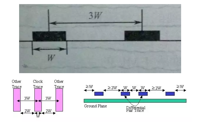
Fourth, electricity formation is not only thermal relief,but also wire.

Because electricity formation is designed to the power of mode of thermal relief,the formation and the image on the actual printed board is contraty. All connections are isolated lines, so be careful when draw several groups of power or separation line,and can not leave a gap,which make two groups power short circuit.

Fifth, the character is misplacing

Character covers pad and SMD lug which cause the inconvenience for tesing the PCB and welding the components.The size of desighed character is too small, resulting difficulties in a screen printing , but if it is too much ,the character will overlap, and it is difficult to distinguish.

Six,the PAD of surface mount device is too short

This is for a continuity test, for too intensive surface device, the spacing between its feet relatively is small,and the pad is also very fine.When install test needle,it must stagger up and down position.If the pad design is too short,it though does not affect device installation,but it will make the test pins are not open.

Seven, settings of sided pad aperture

Sided pads are generally not drilled,if it need to be drilled,it should be labeled,and its aperture should be designed to be zero. If we design the value, so when generating drilling data, this position appeared hole coordinates, and problems appear. If sided pads need to be drilled, it should be marked .

Eight, overlapping pads

In the drilling process several drilling holes in one place will result in damage of the hole bit and the holes. In multilayer board, two holes overlap, after the drawn film ,it is showed the separation disk,which resulting in scrap.

Nine, too much filler block or filler block is filled with fine line in design

Generating the loss of gerber data , or gerber data is incomplete. Because when the plot data is processing,the block is filled by drawing with lines one by one,which cause a large amount of plot data ,and increase the difficulty of data processing.

Ten, the abuse of a patterned layer

made some useless connection on some graphics layer .It is originally four-layer board,but was designed more than five layers,which cause the misunderstanding,and violate the conventional design.In design,it should maintain complete and clear of graphics layer.

Leave a comment

Practical skills summary of high frequency PCB design

16060301_pcb.webp
PCB design goal is smaller, faster and lower cost. And because the point of interconnection on the circuit chain is the weakest link, in RF pcb design, electromagnetic properties at the point of interconnection is the main problem faced by the engineering design, to examine each of the points of interconnection and to solve existing problems.

Interconnection of circuit board system comprises three: a chip to a circuit board, interconnects within PCB board and signal input / output interconnect between the PCB and the external device . This paper describes practical skills summary of high frequency PCB design with the nterconnects within PCB board.I believe that by understanding this paper will bring convenience to further PCB design.

In PCB design,chip and PCB interconnect are important for design, but the main problem between chip and pcb interconnect is that too high interconnection density will lead to that the basic structure of PCB material becomes the factor that limit the interconnection density growth.This article shares practical tips of high frequency PCB design.

For high-frequency applications,techniques of interconnect within the high frequency PCB design include:

1, the transmission line use a 45 ° angle to reduce the return loss;

2, Use high-performance insulation board of insulation constant value which are tightly controlled by levels.This approach is conducive to the effective management of electromagnetic field of the insulating material and the near wiring.

3, to perfect specifications of the high-precision etched PCB design,we should consider total error of required line width is +/- 0.0007 inches;that we should manage the undercut and cross section of wiring shape;that we specify plating conditions of the wiring side wall. The wiring geometry and the surface of coating are overall managed,which is very important for solving the skin effect which is related with microwave frequency and for implementing these norms.

4, highlight lead present tapped inductor,which should avoid the use of leaded components.In high frequency environment, it is best to use surface mount components.

5,For the signal vias,it should avoid using the PTH process on the sensitive plate. Because this process can lead to lead inductance on PTH .If a through-hole on a 20-layer board is used to connect the first layer to the third layer,lead inductance can affect 4-19 layers.

6,we should provide a rich ground layer. We can use molded hole to connect the ground layer , to prevent three-dimensional electromagnetic field affect the circuit board.

7. To select the electroless nickel plating or gold plating process, do not use HASL plating method. This can surfacely provide better plating skin effect of high frequency current. In addition, this high weldable coating requires less lead and help reduce environmental pollution.

8, the solder resist layer prevents the solder paste flowing. However, since the uncertainty of the thickness and unpredictability of the insulating properties make the entire surface of the board covered with a solder resist,which will result in large changes of electromagnetic energy in the design of microstrip . Commonly solder dam is used to make the solder resist layer.

The above is for everyone to share high frequency PCB design techniques in the PCB board interconnect.If you are familiar with these methods, we can understand the use of copper backed coplanar microstrip design is more economical and practical than stripline design.

Leave a comment

8 need-to-know Errors of PCB design

16060201_pcb
We often find some rules or principles that we take for granted will be some errors. Electronic engineers in pcb design will have such examples. The following eight errors are a summary of an engineer.

Error 1: requirement of PCB board design is not high,so use a little fine line, and do the routing automatically.

Comments: The automatic routing is necessary to occupy a larger area of PCB, while it generate more times vias than manual routing. In large quantities of products,factors ,which PCB factory consider for reducing price ,in addition to the commercial factor,are line width and the number of through holes,which are affecting the yield of PCB and consumption of PCB drill.Saving the cost of the supplier also finds a reason to cut prices.

Error 2: These bus signals are used resistance to pull, and feel more ease

Comments: The reasons for the drop-down signal and the drop-up signal are many, but not all have to pull.Pulling a mere input signal need the current of tens of micro amps or less.But pulling a driven signal need milliamps.If pull all the resistance, a few watts of power consumption are all in the resistance.

Error 3: how to handle I/O port that CPU and FPGA can not use? Let it empty now, maybe better.

Comments:if unused I / O port is vacant, subject to outside a litter interference,it may become the input signal of repetitive oscillation , while the power consumption of the MOS device depends on the number of times of turns. If you pull on it, every pin will have microampere currents, so the best way is to set to output ,and of course, there is no other driven signal outside.

Error 4: The FPGA left too much gate to use up, you can enjoy the play.

Comments: The power consumption of FGPA is proportional to the number of triggers used and the number of turns,so the power consumption of the same type of FPGA may vary by 100 times in different circuits at different times . Minimizing the number of high-speed triggers is the basic method to reduce FPGA power consumption.

Error 5: the power consumption of these small chip is very low,so do not consider them.

Comments: It is difficult for less complex internal chip to determine power consumption.It is mainly determined by the current on pin.A ABT16244, if there is no load ,its power consumption is less than about 1 mA,but its indicator is that each pin can drive 60 mA of load (such as matching tens of ohms),namely full load power consumption is up to 60 * 16 = 960mA, of course, it is just the supply current, and the heat fell on the load .

Error 6: memory has so much control signal. I only need OE and WE signal on this board ,so chip select can connect the ground,so that we read out data faster.

Comments: the power consumption of most memory with effective chip select is more than 100 times than that with ineffective chip select.So it should be possible to use CS control chip,and in the case of meeting other requirements, we should try to reduce the width of the chip select pulse.

Error 7: why do these signals have overshoot? As long as the match is well, it can be eliminated

Comments: In addition to a small number of specific external signals (such as 100BASE-T, CML),there all have overshoot.If it is not great, it is not necessary to match. Even if you want to match,it is not necessary to match the best. Like TTL ,its output impedance is less than 50 ohms, or 20 ohms.If so big matched resistance is also used,the current is very large,and the power consumption is unacceptable.While the amplitude of the signal will be too small to be used.Besides output impedance when general signal output the high level is not the same when general signal output the low level.There is no way to do an exact match. So for the match of the TTL, LVDS, 422 ,juts do as the overshoot can be acceptable.

Error 8: reducing power consumption is the matter of hardware personnel , and the software does not matter

Comments: Hardware just take a stage, software is singing . Software amost controls visit of every chip and turns of every signal.If the software can reduce the external memory access times (multi-use register variables, multi-use internal CACHE, etc.),it will contribute greatly to reduce power consumption.

Leave a comment

Refuse rework! 5 golden rules of PCB design

PCB circuit board is the basal electronic components in all electronic products. As the main support, it is equipped with all the devices composed the circuit. PCB role not only combines scattered element, but also ensure the rules of the circuit design,which is good to avoid the confusion and error artificial phenomenon caused by manual cables and wiring.

This paper has detailed description for 5 key design points of PCB in the design of power.

1, To have a reasonable direction

Such as input / output, AC / DC, strong / weak signal, high / low frequency, high pressure / low pressure. Their trend should be linear (or separation), and shall not interacting with each other. Its purpose is to prevent mutual interference.

The best direction is a straight line, but generally it is not easy to achieve.The most unfavorable trend is endless, but fortunately you can set isolation to bring improvement. Requirements of DC, small signal, low-voltage PCB design can be lower. Therefore, the “reasonable” is relative.

2, Choose a good ground: ground is often the most important

The small ground, I wonder how many engineers have done exposition about it,which shows its importance.Under normal circumstances,there is requirement of common point.

In reality, due to various constraints it is difficult to completely do it, but should try to follow. This problem is quite flexible in practice, everyone has their own set of solutions.The explanation for specific printed circuit board is easy to understand.

3, Rational arrangement of power supply filter / decoupling capacitors

In general,if you only just draw a number of power filtering or decoupling capacitors in schematic diagram , but can not point out where they should be connected. In fact, these capacitors are designed for switching devices or other components that need filtering or decoupling capacitors.The arrangement of these capacitors should be as close to these component parts.If they are too far, they do not work.Interestingly,when the arrangement of power filtering and decoupling capacitor is reasonable,the problem of ground is not obvious.

4, Lines have requirements,and the size of buried holes and vias is appropriate .

Lines,which have the condition to be made wide, are never made fine. High-pressure and high-frequency lines should be sleek,and should not have sharp angles and corner ,so should not use the right angles. Ground should be as wide as possible, it is best to use a large area of copper, which has great improvement for ground point. The size of PAD or thread holes is too small,or pad size and drilling size mismatch.The former is unfavorable for manual drilling,and the latter is unfavorable for CNC drilling .The pad is easy to drill into “c” shape, if redrilling, the pad easily be off.

Wire is too small, and a large area of the unwiring region is not set with copper, which is likely to cause corrosion uneven. That is when the unwiring region finish etching,fine wire is likely to corrode too far,or a non-broken off, or completely off. Therefore, the role of setting copper does not just increase ground area and immunity.

5, the solder joints of vias and wire density

Some problems at the beginning of the production of the circuit is not easy to be found. They tend to emerge in the late, for example, there are too many via line.If the plating process has any carelessness,the hidden trouble will appear. Therefore, the design should minimize the thread hole.

The density of Parallel lines is too large, it is easy to welding together.Therefore, the line density should be determined according to the level of welding process.If the solder joint is too small,it is not conducive to manual welding.Welding quality can only be resolved by reducing the efficiency,or it will leave hidden trouble.Therefore, to determine the minimum distance from the pad should consider the quality and efficiency of welding personnel.

If we can fully understand and master the above considerations of PCB design , it is possible to greatly improve the design efficiency and the pcb manufacturing quality. When in production correcting the existing errors, we will be able to save a lot of time and costs, and save rework time and material inputs.

Leave a comment

3W principle of PCB design

In the PCB design ,in order to reduce crosstalk between lines, we should ensure line spacing is large enough.When the distance between the line center is not less than three times than line width,you can keep most of the electric field noninterference,which is 3W principles.

As shown below: meeting 3W principle enables crosstalk between signals reduced by 70%, and meeting the 10W enables crosstalk between signals reduced by nearly 98%.

16060303_pcb

3W principle is although easy to remember, but to emphasize that this principle with previous condition is established.Considering physical significance of the causes of cross talk,in order to effectively prevent cross talk,the spacing is related with stack height and line width. For the four-layer board,the distance between traces and the reference plane height (5 ~ 10mils), 3W is enough; but for two-layer board,the distance between traces and the reference plane height (45 ~ 55mils),3W may not be enough for high-speed signal traces .3W principle is generally established at he conditions of 50 ohm characteristic impedance transmission line.

3W principle is that when a plurality of high-speed signal has long-distance traces,its spacing should follow he principle of 3W, such as a clock line, differential line, video, audio signal line, a reset signal line ,and other critical systems which need to follow the circuit 3W principles,not all the wiring on pcb board must enforce compliance with the principle of 3W.

Leave a comment

Shielding method of high-speed PCB design

Transfer rate of high-speed PCB design wiring system is steadily accelerating, it also brings a certain anti-interference vulnerability.This is because the higher the frequency of the transmission, sensitivity to signals increase, while their energy is increasingly weak. At this point wiring system is more susceptible to interference.

high speed pcb design

high speed pcb design

Interference is everywhere.Cables and equipment will cause the interference for other components or serious interference by other sources.such as: computer screens, mobile phones, electric motors, radio broadcasting equipment, data transmission and power cables.In addition, potential eavesdroppers, hackers and cyber crime are increasing because they intercept UTP cable information transmission which can cause tremendous damage and loss.

Especially when using high-speed data network, the time of intercepting a lot of information is significantly lower than the time of intercepting low-speed data transmission.

Faraday shield

The role of cable shield is like a Faraday shield.The interference signal will enter into the shield,but can not enter the conductor. Thus, the data transfer can be trouble-free operation. Since the shielded cable has a lower radiation sporadic than unshielded cable ,which prevent the network traffic was blocked.

Shield select interference fields of different interference fields are mainly two kind:electromagnetic interference and radio frequency interference. Electromagnetic interference (EMI) is mainly low frequency interference.Motors, fluorescent lights and power lines are the usual sources of electromagnetic interference. Radio Frequency Interference (RFI) refers to radio frequency interference, and it is mainly high-frequency interference. Radio, television, radar and other wireless communications are the usual sources of RF interference.

For resistance to electromagnetic interference, selecting the braided shield is most effective because it has a lower critical resistance; for radio frequency interference , foil layer shielding is the most effective, because the braided shield depends on the change of the wavelength . The gap it produces make a high-frequency signal freely in and out conductor; and for mixing high and low frequency interference field, we will have to use a combination shielding method of braid and foil layer with broadband coverage function. Generally, the higher the mesh shield coverage is, the better shield effect is .

Leave a comment

The introduction of special board plating methods in PCB manufacturing

This paper mainly describes four special plating method of the circuit board manufacturing

pcb manufacturing

pcb manufacturing

The first kind, refers to the row type electroplating.

It often requires rare metals plated on edge-board connector, edge-board protruding contacts or gold finger,in order to provide low contact resistance and high wear resistance.This technology is called row type plating or projection plating.Often plate gold on the protruding contacts of the edge-board connector whose inner plating layer is nickel. Goldfinger or edge projection use the manual or automatic plating technology.Currently gold on the plug or gold finger has been replaced by rhodium plated, lead plated . The process is as follows:

1) stripping coating and removing tin or tin-lead coating of protruding contacts .
2) Rinse with cleaning water
3) Scrub with an abrasive scrub
4) Activation is immersed in 10% sulfuric acid
5)plate nickel on protruding contacts in the thickness of 4 -5μm
6) Cleaning demineralized water
7) Treatment of gold osmotic solution
8) Gold Plated
9) Cleaning
10) Drying

Second, through-hole plating

There are multiple ways to build a plating layer that can meet the requirement on the hole wall of the drilling hole of the base plate,which is called the activation of walls in industrial applications.PCB manufacturers need a plurality of intermediate slot to produce.Each slot has its own control and conservation requirements.

Through-hole plating is follow-up necessary production process in the process of drilling.When the drill bit drills through the copper foil and the underlying substrate, the heat generated makes insulating synthetic resin which form the majority of substrate melt. The molten resin and other drilling debris accumulate around the hole,and coat on the new exposed hole wall in the copper foil,which is in fact detrimental in the following plating surface. Molten resin will leave heat axis on the hole wall of substrate,which exhibite poor adhesion for most of activator,which requires the development of techniques that is similar to the stain and etch back chemistry.

A method ,which is more suitable product for pcb prototyping, is to use a low-viscosity inks that is specially designed,which is used to form high-adhesive and high-conductive coating film on each through-hole wall.This do not need to use multiple chemical processes ,only one application step, followed by heat curing, which can form continuous coating film in all the inside hole wall .it does not need further processing and can be directly plated.

This ink is a resin-based material.It has a very strong adhesion. It can effortlessly adhere on most polished hole wall,which eliminate the etch-back step.

The third, roll wheel gearing type selective plating

Pins of electronic components, such as connectors, integrated circuits, transistors, and a flexible printed circuit circuit and so on,are all used the selective plating to obtain a good contact resistance and corrosion resistance.This plating method can be used manually, or automatically .The individual selective plating for each pin is very expensive, so you must use mass soldering.

Typically,punch both ends of metal foil whose thickness is required by being flatted.Do the cleaning by chemical or mechanical methods,then selectively use the nickel,gold, silver, rhodium, or tin-nickel alloy, copper-nickel alloy, and nickel lead alloy to continuous plating. In the method of selective plating,firstly,the part which does not need to be plated on the metal copper plate is covered with resist film.Only partly plate in selected copper.

Fourth, brush plating

Another selective plating method is called ” brush plating”.It is an electrode position technique. Not all parts are immersed in an electrolyte during plating.
In this plating technique, only a limited area is plated, but it has no effect on the rest. Typically, make the rare metal plated in selected portions on printed circuit board , such as edge-board connectors .

Brush plating is used more time when maintaining waste printed circuit boards in the electronics assembly workshop. A special anode (chemical reaction is inert , such as graphite) is wrapped in absorbent material (cotton swabs), and use it to bring the plating solution to the required plating place.

Leave a comment

The interpretation of common nouns in PCB Manufacturing and Design

The assembly layer is used to represent the physical size of the device.It can be used when the mounter is welding.
Assembly layer can put a nominal value of the device, such as the value of resistance and capacitance .This is very convenient to assembly maintenance .

We will certainly encounter solder Mask and paste Mask when drawing the PCB design. Previously we vaguely are aware that solder Mask is a solder layer, a solder paste layer is a paste Mask.We do not care about it when using the protel.But when we use the cadence,it needs ourselves to make the PAD,so we must know the meaning of the two.

Solder Mask Layer: this is the reverse layer ! Some means nothing, and nothing represents there!

Solder mask is the place where is coated with green oil except the PAD(surface mount pads, plug-pad, via),which is to prevent the place where should not be tin-plated from being tin-plated when PCB is though the tin stove, so it is called solder mask layer or green oil layer.I think people who have seen the PCB should see this green oil.Solder mask can be divided into Top layers and Bottom layers.PAD should be exposed in solder layer.This is small circles or small square circle which we can see when we only display the solder layer,generally larger than PAD.Solder surfacely means solder mask layer,which is used to coat with solder material, such as green oil,to prevent the place where should not be welded from being tin-plated.This layer will expose all the PAD that is need to be welded, and the openings are bigger than the actual PAD.When generating the Gerber file,you can observe the actual effect of solder layer.When you draw a rectangle in solder masks layer which has top solder and bottom solder,the position in the rectangular frame is equal to openning window,where is not need to be coated with oil,where is the shiny copper.Solder Mask is painted green oil, blue oil, red oil, in addition to the welding plate and via which are painted, they will not be tinplated. Other should be coated with solder resist.And this solder resist has the colour of green,blue. red and so on.When painting cadence pads, solder Mask pad is larger 0.15mm (6mil) than regular pad .

Paste Mask layers [solder Paste protective layer] :this is positive.Some represents there and nothing is nothing.

It is for the components of SMD.This layer is used to make steel film .While the holes on the steel film correspond with the pads of SMD devices on the circuit board.When welding SMD,firstly make the steel film cover on the PCB (corresponding to the actual pad),then coat with paste.Scrape off the excess paste with a doctor blade and remove teh steel film,which makes the pad of SMD device tin-plated.Then make the SMD device attached on the paste by manual or machine.After the rellow,the welding the SMD device is finished. Usually the holes on the steel membrane is smaller than actual pad on the PCB printing.By specifying an extension rule to zoom in or out the protective layer of solder paste. For the different requirements of different pads, you can also set multiple rules on paste protective layer. The system also provides two solder protective layer, and they are top paste protective layer and bottom paste protective layer.When you draw a rectangle in paste mask layer which has top paste and bottom paste,the position in the rectangular frame is equal to opening window,and the machine sprays tin within this window .

Meanwhile Keep-out and Mechanical layer are also very easy to confuse., Keep-out is a painting frame, which determine the electrical boundary.

Mechanical layer is real physical boundaries. Positioning holes are made according to the size of Mechanical layer.But the PCB factory engineers generally do not understand this.So it is best to delete keepout layer before sending to PCB factory.It was occurred in the laboratory that PCBfactory has wrong cut of boundary because of not deleting the Keep-out layer.

We often encounter assembly layer and the printing layer in the PCB Gerber file. So what is meaning of the two layers?

Silkscreen: a plan view of the shape of the part.The silkscreen layer is the graphic symbols that are representative of device profile.When designing the PCB , the plot data often use this layer data. More appropriate to say that Silkscreen layer will be printed on the PCB board.

Assembly layer: PLACE BOUND TOP/BOTTOM, namely physical sharp graphics.It can be used in rules of DFA. DFM is short for “Design for manufacturing”.DFA is short for “Design for Assembly”This property is used to the layout and the assembly drawing.

We also often meet with the two words: positive and negative in the PCB . Positive and negative only refers to two kinds of different display effect on one layer.Whether this layer you set is positive or negative,the printed PCB board is the same.Just in the processing of the cadence, data volume, DRC detection, and the process of the software are different。Only one thing with two kinds of expression. Positive is that what you see is what you see.Wiring you see is the wiring.It really exist.Negative is that what you see, there is nothing.What you see is just the copper that is needed to be etched.

Positive film has the advantage that if we remove the components or vias, we need to shop the copper, and we have more comprehensive DRC check。Negative is the advantage that if we remove the components or vias, we do not need to shop the copper, and copper shop is automatically updated.But we have no comprehensive DRC check。

In the painting via pad ,holes are bigger 10mil (0.2mm) than the pin.Outer diameter is larger more than 20mil than holes, or the pad is too small and welding is inconvenient.

Leave a comment

Grid settings Skills in the PCB design layout

First, PCB design requires different grid settings at different stages.

A large grid point can be used for component layout in the layout stage。

For IC, non-locating connectors and other large components, you can use the grid point accuracy 50-100mil for the PCB layout, and for resistors and capacitors and inductors and other passive small components,you can use 25mil grid for layout. Precision of large grid point contributes to the alignment of components and the beauty of layout.

PCB layout rules:

1, under normal circumstances,all the elements should be arranged on the same side of the PCB board.Only the top element is too close , some of the highly limited and small heat device, such as chip resistors, chip capacitors, stickers chip IC, etc. can be arranged on the lower level.

2, on the premise of ensuring the electrical performance, the element should be placed on the grid and arranged parallel or perpendicular to each other, in order to clean, beautiful, In general,overlapping elements is not allowed.Elements are arranged to be compact.The element should be uniform distribution and consistent density on the entire plate.

3,The minimum spacing between adjacent land pattern of different components on the circuit board should be more than 1mm.

4, The distance from the edge of the PCB board is generally not less than 2mm. Best board shape is rectangular .Aspect ratio is 3: 2 or 4: 3 .When the size of the printed circuit board is greater than 200MM by 150MM,we should consider the board can sustain mechanical strength.

Second, in the PCB design layout, we should analyze the circuit board unit, according to the function to layout design.

The layout of all the components of the printed circuit board should comply with the following principles:

1, according to the process of the circuit ,arrange the position of the respective functional circuit elements which enable the layout is easy to the signal flow and make the signal a consistent direction as far as possible.

2, centering on the core components of each functional unit ,around which to layout.Components shoulde have uniform ,integral,and compact arrangement on the PCB.we should minimize and shorten the lead and the connection between the various components as far as possible.

Leave a comment

Necessary knowledge of PCB design _ specifications of PCB layout and design

We all know that “nothing can be accomplished without norms or standards”, the technology too. What specification should pay attention to when designing PCB ?

1. layout design specification

A,The distance to edge should be greater than 5mm or 197mil

B, first place the components that is close to the structure, such as connectors, switches, power sockets, etc

C, priority put core components of circuit function block and large components, and centering on the core components ,placed around the circuit components

D, components with large power are put in the position that is conductive to heat.

E, components with larger quality should be avoided on the center of the board,and should be putted close to the fixed boundary of the case.

F,components with high frequency connection should be as near as possible, to reduce the distribution of the high frequency signal and electromagnetic interference.

G,components of input should be away from components of output as far as possible .

H, components with a high voltage should be putted where the hand is not easy to reach when debugging.

I, thermal element should be far away from the heating element

J, adjustable components layout should facilitate of adjustment

K, considering the signal flow, layout with reasonable arrangement makes signal flow as consistent as possible

L, layout should be uniform, neat and compact

M, for SMT components, consistency of solder direction should be paid attention,which is good for PCB assembling and welding,and reduce the possibility of bridging.

N, decoupled capacitor should be at the location of the nearest power input.

O,the height of wave soldering components is limited 4mm.

P, for the PCB with double-sided components, IC with the larger density and plug-in components should be putted at the top of PCB board.Small components and SMD components with less pin and loose arrangement can only be putted at the bottom of board.

Q, adding the radiator for components with small size and high heat is particularly important.High power components can be heat dissipation by bonded copper, and try not to put heat sensitive components around these components .

R, high-speed element should be close to the connector as near as possible;
Digital circuit separate with analog circuit as far as possible.It is best that they are divided and single point grounding.

S, the distance between positioning hole to the nearby welding plate is not less than 7.62 mm (300 mil).The distance between positioning hole to surface mounting components is not less than 5.08mm(200 mil).

2 .wiring PCB design specification

A, line should avoid acute Angle, right Angle.Forty-five degrees should be used to trace.

B,signal lines of adjacent layer is the orthogonal direction

C, the high frequency signal is as short as possible

D, input and output signal as far as possible to avoid adjacent parallel lines.It is better to add ground wire between lines, in case of the back coupling.

E, the power cord of double-side board ,it is better that ground wire is consistent with the data flow direction, in order to enhance ability to resist noise.

F, digital and analog need to separate
The clock line and high frequency signal lines should consider line width according to the characteristic impedance requirements, to achieve the impedance matching

G, the wiring and drilling should be uniform in the whole circuit board .

H, The separate power layer and ground layer, the power lines and ground wire should be as short and thick as possible.Loops composed of power and ground should be as small as possible.

I, clock wiring should drill less holes, and try to avoid parallel lines with other signal lines,and should be far away from the general signal line, to avoid the interference to signal lines;At the same time avoiding the power part on the plate, to prevent mutual interference between power and clock;When a piece of circuit board has a number of different frequency clock, the clock line of two different frequency can not be parallel lines .The clock line should avoid close to output interface, to prevent high frequency clock coupled to the output CABLE line and launch out;If boards have special clock chip, its lower parts cannot place the line.Its lower part should be spread copper.If necessary , special cede territory for it;

J, paired difference signal lines generally parallel to the line, trying to drill a hole.If necessary,two lines should be drilled together, to achieve the impedance matching.

K,the space between two solder joint is very small, adn solder joint may not be directly connected ;Through-holes from the paste disc should be away from the PAD.