Leave a comment

Two great tips of PCB software CAM350

CAM350 is the industry standard for PCB verification, optimization and output generation to efficiently and effectively drive PCB fabrication.

More and more complicated PCB designs require comprehensive verification before they are transferred to the PCB manufacturer to ensure a perfect and timely produce of bare PCB boards. Problems emerging during the PCB manufacturing can effect the product schedules, result in costly design re-spins, and require modifications to the design that might compromise the PCB design’s intent and integrity . Inspecting, preparing and validating the PCB design before releasing to manufacturing will lead to a vital increasement in efficiency, less risk of design re-spin, and, most importantly, successful electronic products, faster time-to-market, but at less cost.

CAM350 provides a full suite of tools, from design through production, streamlining the transition of PCB design data into right and real PCBs. following are two tips of CAM350 helping the customer to master this great tool.

When the text layer in some PCB Gerber data has a lot of text box,and the distance between text box and PAD can not meet the process capability.When the Gerber data has a large area of copper foil cover, the distance between lines or PAD and copper is beyond to the production requirements, and the outline size is big…You can draw on the experience of treatment methods of this article.

One,When the Gerber data has a large area of copper foil cover, the distance between lines or PAD and copper is beyond to the production requirements, and the outline size is big,you can use the below method to rapidly trimming the distance between lines or PAD and copper.

1, Copy all the PAD in the circuit layer( this is the first layer) into an empty layer.Delete the corresponding PAD on the copper sheet and enlarge the rest PAD as a reduction of the line layer(that is second layer).

2, then copy the first layer into an empty layer.Delete the copper sheet as third layer.Combination way is: the first layer , the second layer , the third layer.

In general, in order to reduce the amount of data, we can keep only copper sheet the first layer .If only the distance between welding to copper sheet is not enough,you can copy the welding layer that is enlarged and can meet the process capability into an empty layer.Delete the correspongding sold mask on copper sheet, and enlarge the rest sold mask as second layer.

Note: after using this method to completes the circuit, be sure to use the order: Utilities–>Convert Composite to convert multiple layers into composite,and change this composite to one layer.And then use the order:Anglysis–>Compare Layers to check this layer with original layer carefully .

Two, when the text layer in some Gerber data has a lot of text box,and the distance between text box and PAD can not meet the process capability,you can draw on the experience of below methods :

1, Use the order:Edit–>Move Vtx/Seg to stretch the text box up to specifications,and then make it flash.

2, then make the other text box of the same type the same flash.But note that after making it Flash ,the flash must be broken up, in case of rotation of D date when openning the data next time.

Leave a comment

Little PCB knowledge – the relation between ounces and thickness of bonded copper

Today we going to share the pcb knowledge about the copper thickness unit, which should be usefull for the new PCB designers.

The thickness of 1 oz is about 35 um.

1 oz mean weight of the average copper foil in the area of 1 square foot is 28.35g, which use the the weight of unit area to represent the average thickness of copper thinness.

Conversion methods:

1 square foot = 929.0304 square centimeters,

The copper foil weight divided by the density and the surface area,that is the thickness of copper foil!

The density of Cu = 8.9 kg/dm ^ 3

Copper thickness is T

Tx929.0304 square centimeters x8.9 g/cm3 = 1 oz = 28.35 g/cm2,

T = 0.0034287 cm = 34.287 um

The relation between PCB line width and the current

One, the calculation method is as follows:

First calculate the Track sectional area.Most of the copper foil thickness of the PCB is 35 um (if the copper thickness is not sure,you can ask your cooperated PCB manufacturer).The copper thickness multiplied by the line width is the cross-sectional area.Pay attention to the conversion into square millmeter.Experience value in a current density v is 15 ~ 25 amps/mm2.The experience value multiplied by the sectional area is capacity.

I = KT0.44A0.75

K means the correction coefficient.It takes 0.024 when the copper wire is in the inner layer.And it takes 0.048 when the copper wire is in the outer layer.

T means the maximum temperature rise,and the unit is degrees Celsius (copper melting point is 1060 ℃)

A means cross-sectional area of copper, and the unit is square MIL (not mm , pay attention to square MIL.)

I means allowable maximum current, and the unit is the ampere (amp)

Generally, 10 mil = 0.010 inch = 0.254 ,which can be 1 A.250 mil = 6.35 mm, which can be 8.3 A

Two, the data:

The calculation of PCB current-carrying capacity is always lack of authoritative technology method and formula. Experienced CAD engineers rely on personal experience to make more accurate judgment.But for CAD novice, it meets a difficult problem.

PCB current-carrying capacity depends on the following factors:line width, line thickness (copper foil thickness) , the permissible temperature rise.As everybody knows, the wider PCB line is, the greater the current-carrying capacity is.Assuming that under the same conditions, 10 mil line can withstand the 1 A, then how much current can 50 mil line withstand? Is it 5 A?Naturally the answer is “no”.Please see the following data from the international authoritative institutions :

The unit of line width is Inch ( 1 Inch = 25.4 millimetres ) 1 oz copper = 35 microns thickness, 2 oz. = 70 microns thickness, 1 oz = 0.035 mm, 1 mil = 10∧-3 Inch.

In experiments, the length of wire line causes the line resistance that causes the pressure drop,which has to be considered.Tin in the process is just to increase the current capacity,but it is hard to control the volume of the tin.1 OZ copper and 1 mm width, usually 1-3 A . Specifically see your line length and the requirements for the pressure drop.

The maximum current value should mean the maximum allowable value under the temperature limit.Fusing value is the value of copper melting.Eg. 50 mil 1 oz temperature 1060 degrees (i.e. copper melting point), the current is 22.8 A

Safe current of aluminium wire is 4-5 A per square millimeter

Safe current of copper wire is 5-6 A per square millimeter

The copper wire of maximum current can run 10A with one square millimeter.

The relationship between sectional area of wire and the current

Safety calculation method of copper wire is as below:

The safe current-carrying capacity of copper power wire of 2.5 mm² is 28A

The safe current-carrying capacity of copper power wire of 4 mm² is 35A

The safe current-carrying capacity of copper power wire of 6 mm² is 48A

The safe current-carrying capacity of copper power wire of 10 mm² is 65A

The safe current-carrying capacity of copper power wire of 16 mm² is 91A

The safe current-carrying capacity of copper power wire of 25 mm² is 120A

If it is aluminium wire, wire diameter is 1.5 -2 times of copper wire.

If the current of copper wire is less than 28 A, 10A per every square millimeter is safe .

If the current of copper wire is larger than 120A, 5 A per square millimeter is OK.

The current that can normally go through the sectional area of the wire,has a choice according to the sum of needed current.

The aluminum wire below 10 mm², square millimeter number multiplied by five is ok, if the copper wire,rose up a gear

The copper wire of 2.5 square, is calculated at four square. More than one hundred ,they are all cross-sectional area multiplied by 2.

Under 25 square,multiplied by four,

More than 35 square, multiplied by three

70 and 95 square,multiplied by 2.5

Note: it is only as estimation.It is not very accurate.

In addition ,if the copper wire is less than 6 mm² in indoor electronic wire,it is safy that every square current is not more than 10A.From this perspective,you can choose copper wire of 1.5 square or aluminium wire of 2.5 square.

Within 10 meters,the wire current density of 6A is more appropriate.

10 to 50 meters, 3 A/mm²,

50-200 meters, 2 A/mm²,

More than 500 meters, less than 1 A/mm².

From this point of view, if it is not far away, you can choose copper wire of four square or aluminum wire of 6 square.

If that’s the distance of 150 meters of power supply (it is tall buildings or not),copper wire of four square must be adopted .

The impedance of the wire is proportional to its length, and is inversely proportional to the wire diameter.Please use power with special attention to the wire and wire diameter of the input and output wire.In order to prevent the accidents caused by overheat line because of the too big current.

Leave a comment

Application of digital ink-jet printing technology in the PCB manufacturing

Use digital link-jet printing technology to develop and produce PCB, which can positively simplify the production process and shorten the production cycle; which greatly reduce the expensive production equipments and save the cost. It greatly reaches the goal of “energy conservation and emissions reduction”, especially for reducing the capacity of waste-water and improving the environmental pollution, move to “green production”. Therefore, “digital ink-jet printing technology” will get rapidly promotion and application in the PCB industry, and will become the mainstream in PCB manufacturing!

Following is the overview of the ink-jet printing technology from three aspects:

1. Application of digital ink-jet printing technology in PCB industry

“Digital ink-jet printing technology” has mainly four aspects of the application in PCB industry:

(1) Using digital ink-jet printing technology to generate the pattern of corrosion or plating resistance. Using this technology can reduce more than 60% production process of traditional “pattern transfer” process,and can save about 60% of the ink and dry film,and can decrease more than 60% of organic wastewater treatment and discharge.
(2) Applying “digital ink-jet printing technology” to form solder mask and legends. Adopting this technique can reduce more than 60% of the production process of traditional solder mask and characters, and can save more than 50% of solder mask ink,and can reduce more than 60% of organic wastewater treatment and discharge,and can improve the product percent of pass and shorten the production cycle, to reduce the cost of solder mask.
(3) Adopting “digital ink-jet printing technology” produce PCB products directly.The flow is: jet printing conductive graphics on the base material——low temperature sintering——jet printing medium layer——jet printing plating through holes——low temperature sintering——jet printing conductive graphics, repeating the processes to form the required “laminated board”.

Of course, the application of “digital ink-jet printing technology”, needs to follow the development rule of all things,from small to large, from weak to strong, from local to overall, from low level to high level.Therefore, it has to be from the first application in “corrosion or plating resistance” and solder mask and legends,and then to the full jet printing technology based pcb products .

2. key equipment and materials

(1) key equipment – “digital-control” inkjet printer. Including: i). the print head, can spray 5 to 50PL of link drops. ii) productivity, can satisfy the PCB mass production requirements. For example, the working time of 20 x24 square inch working in process board should be between 20 to 60 seconds.
(2) the key materials: printing ink.
The ink usd for ink-jet printing is different from the conventional ink ,especially the viscosity and thixotropy.For the conductive ink used in the PCB production which fully adopt “digital ink-jet printing technology”,must be the ink of “nanoscale metal particles (such as silver, gold, copper, etc.)” , to ensure the sintering under the condition of low temperature , and achieve the conductivity of the metal conductor.

3. Current situation

At present, Japan and the United States have market-oriented professional digital ink-jet printing and special printing ink.Such as MJ6151 series products of Japan CicroCraft k.k ,and Greenjet series(digital solder mask printing system) products of American Printar Inc. These products can be applied in the large-scale production of 50-150 um wire and all kinds of graphics. “Super” digital inkjet printer and “nano silver ink” and “nano gold ink” have emerged, that is to say, the ink drop of 3-5 PL can be jet-printed ,and wire of 3-30um can be producted.So manufacturing full printed electronic products is getting there!

Must be fully aware that full printed electronic using ink-jet printing technology is great innovation which simplifies the PCB production processes, and reduce the cost and greatly improve the environment pollution and foward the green manufacturing, and is an revolutionary progress of PCB industry

iFastPCB will keep continuous attention on this technology, and will apply it at right time in the future t.

Leave a comment

Vertical Continuous Plating(VCP) line completely defeat traditional plating line to boost the healthy development of PCB manufacturing

With the development of electronic devices toward to diversification of varieties ,functionality and Product minimization, Printed Circuit Board manufacturing industry faces the challenge of more sophisticated equipment and more advanced technologies.

Universe Group ,as professional wet pcb process equipment manufacturer, is facing current challenges and gradually introducing industy 4.0 intelligent production mode. It reserches and developes and make independently the vertical continuous plating line (VCP). Since 2011, just a few short years, VCP sales volume has exceeded 121 lines. It is widely used for pcb manufacturing process such as: panel plating, graphics plating, filling holes or half-filling holes plating, soft board plating and so on.

It is reported, the design concept of the universe group VCP line is updated on the basis of traditional plating line .Compared with traditional plating line, it has more advantages as below :

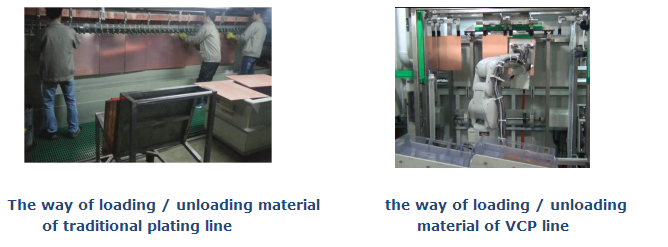
Device of loading / unloading material: the universe group VCP line adopts automatic design of loading and unloading material. The shortest cycle is only 8 seconds.
While traditional plating line can only load and unload the material by manual, which needs more operators, and the labor intensity is high, the staff turnover is fast, which is easy to cause Labour shortages.

Transmission structure: the universe group VCP line adopts transmission way of combination chain type with movable cathode pylons. Pylons drive more smoothly and connectibity is better. it has the advantage of less impact and low noise, etc;

While traditional plating line, impact and noise of bumble motor making serious noise pollution.
PCB_manufacturing_plating line 1

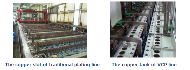
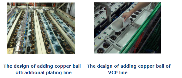
The device of adding copper ball:the VCP line can add copper ball during the PCB production.You can add the copper ball at any time without stopping the machine.This operation is very convenient and the copper ball will not fall into the copper groove .

While traditional plating line needs to stop the machine when adding copper ball, which is extremely unconvenient, and copper ball is easy to fall into the groove. Its efficiency is low and affect the production capacity.
PCB_manufacturing_plating line 3

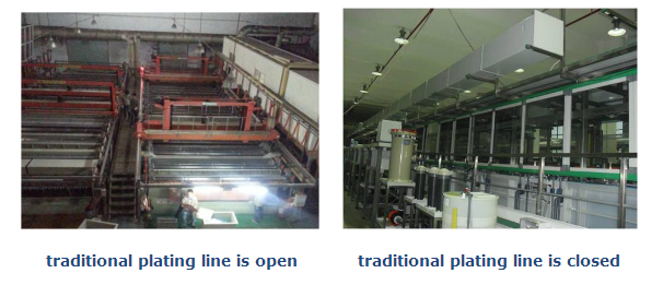
Production environment: in the same capacity, compared with traditional plating ,the contact area between liquid and air of VCP line is smaller,which is only a third of traditional plating line.Using the lateral jet produces less waste gas,so the required pumping air volume is small,and energy consumption is slow.The top extraction design of sealed equipment can greatly reduce gas leaks, which makes work environment safe and comfortable;

While traditional plating line is open.It is difficult for traditional plating line to achieve the effect of VCP in sealing.Because the quantity of copper plating tank is big, and the surface area of exposed liquid in air is much, and pylon has frequent movement which produces a large amonut of waste gas. So the whole workshop has harmful gas,which has serious impact on employee health. The pcb manufacturer need to configure high-power convulsions system to make the environment improve slightly, and energy consumption is high.The conservative estimated enerhy consumption is more than two times than VCP line .
PCB_manufacturing_plating line 4

Process control: the copper tank of the universe VCP line is all connected, and uniform circular, whose tank is equivalent to one copper groove.In process control, only liquid in one copper slot or several copper slot is needed,which is simple and easy to analysis;

And traditional plating line, the number of copper slot is much.The copper tank works alone and does not connect together.In process control,the liquid in every copper tank is needed to analysis,which makes process tedious and big workload.
PCB_manufacturing_plating line 5

Body material: the body of VCP line is made of flame retardant PVC material of V0 class.When in the fire,it most becomes black ,but not burn,which can effectively prevent the fire.The so-called prevention is like that;

While traditional plating line is generally made of ordinary PP material.PP material is not only easy to burn but more help burn. Throughout the fire in PCB factory, it is mostly caused by plating workshop,while the flammable PP material is one of the main culprit causing the fire;

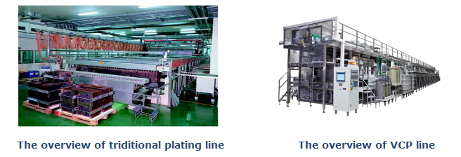
Floor space:the structrure of the VCP line is compact, and the floor space is small ;The universe group has a total four kinds of VCP equipment:
double up-down VCP line(called a DVCP), single up-down VCP line, circular transfer VCP line, one-piece transmission ring VCP line.They can satisfy users of different site conditions,and it is very flexible and convenient;

While traditional plating line, the floor area is larger, and requirements for plant height is high, which is at least 4 ~ 5 meters;Under the same capacity condition,space required by VCP line is only 50% of the traditional plating line, which greatly save space.

Maintenance: the structure of the VCP line is simple, and adopt humanized design with fool proof, and quick release, and color letter management.It is extremely convenient and high efficiency, and it is also easy to achieve 7S standard.

While traditional plating line ,its copper plating tank span is big, and it is easy to cause accident. It often exists environmental problems, and maintenance person need to be down to clean the copper tank, extremely unconvenient. The fixture needs frequent maintenance and repair, and the cost is high.
PCB_manufacturing_plating line 6

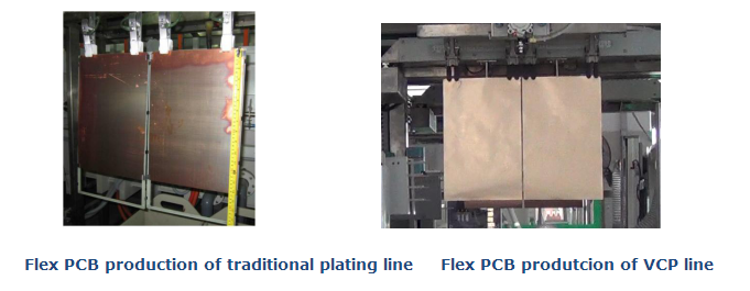
Flexiable PCB production: the VCP line can directly produce the flex PCB board with 0.036 mm thickness or above without the fixed framework; Traditional plating line need the frame during producting any kinds of flex board.
PCB_manufacturing_plating line 7

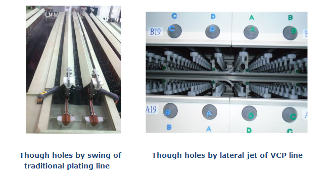
Through-hole ability: the VCP line uses the supercharged nozzle to spray up closely, to strengthen liquid penetration ability, which can meet the demand of HDI PCB production;
While traditional plating line makes the potion into the hole only by soaking and swing. Its strength is small, and penetration ability is limited, so it can only meet the demand of ordinary plate production.
PCB_manufacturing_plating line 8

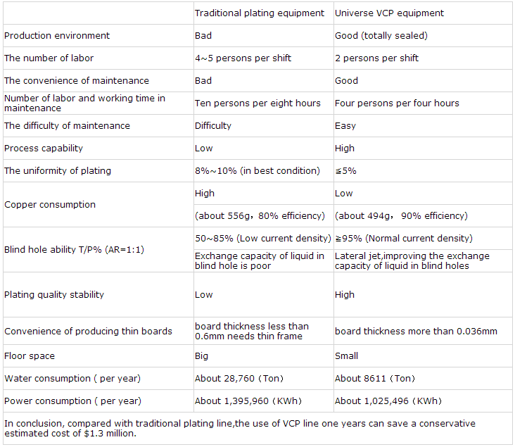
Conclusion: the advantages and disadvantages between VCP line and traditional plating line, as follows:
PCB_manufacturing_plating line 9

Due to the limitations of structure and technology, traditional plating line has gradually lost its competitive advantage.In addition to producing a small part of the high depth of the products,the more cost-effective VCP line will replace the traditional plating line.Universe Group VCP line is a good example of industy.we believe,under the impetus of outstanding enterprise as the universe group, the development or PCB manufacturing industry toward to the sustainable and healthy direction of low consumption, low pollution, high quality, high efficient.

Leave a comment

The introduction of common standard of PCB manufacture and Assembly

The introduction of common standard of PCB manufacture and Assembly

1) IPC – ESD – 2020: Joint standard of electrostaticdischarge controlling program development ,including design, build, implement and maintain of electrostatic discharge control program. According to some experience of the military and commercial organizations, providing guide for processing and protecting of electrostatic discharge in sensitive period.

2) IPC-SA-61A : Post solder semi-aqueous cleaning handbook, including all aspects of Semi-aqueous Cleaning,including chemical and productive residue, equipment, technology, process control and considerations of environment and safety .

3) IPC-AC-62A: post solder aqueous cleaning handbook.Describing PCB manufacturing residue, the types and properties of aqueous cleaner, the process of aqueous cleaning, equipment and processes, quality control, environmental control ,the safety of employees,the test of cleanliness and its cost.

4)IPC-DRM-40E: Through-hole solder evaluation handbook reference.Describing the components,the hole wall,and the welding surface in detail according to the standard requirement.In addition, also including the 3D graphics generated by computer.Covering the filling tin, contact Angle, wetting, vertical filling, welding pad cover and a large number of weld defects.

5) IPC – TA – 722: Solder technology evaluation reference, includes 45 articles of welding technology in all aspects.The content involves ordinary welding ,welding materials, manual welding, batch welding, wave soldering, reflow soldering, gas phase welding and infrared welding.

6) IPC – 7525: template design guidelines.Providing guidelines for the design and manufacture of template for solder paste and surface mount adhesive.Also discussing template design with the application of surface-mount technology.Introducing hybrid technology with through-hole or flip chip components,including the overprint, double seal and phase type template design.

7) IPC/EIA J – STD – 004: requirements for soldering fluxes,contain technical indicators and classification,such as rosin, resin and others.Solding fulxes can be divided into two classes: organic and inorganic flux according to content and activation of halide in fluxes.

8) IPC/EIA J – STD – 005: requirements for soldering pastes,list the characteristics and technical index requirements of solder paste, including test method and the metal content standards, as well as the viscosity, collapse, solder balls, viscosity and wetting properties of solder paste.

9) IPC/EIA J – STD – 006A: requirements for solder alloy of electronic grade,solding fluxes,influx solid solder,provide term name, specification requirements and test methods for electronic grade solder alloy,for flux of bar, strip, and powder, for solding tin of influx, for the application of electronic soldering, for special electronic grade solder .

10) IPC-Ca-821: The general requirements of thermal conductive adhesive.Including requirements and test methods for thermal conductivity of the dielectric that makes the copmonents adhere the suitable location.

11) IPC – 3406: guide of conductive surface coating binder,provides the guide for the secection of conductive adhesive which is as Solder alternatives in the electronic manufacturing.

12) IPC – AJ – 820: handbook of PCB assembly and welding, contains descriptions of assembling and welding inspection technology, including the terms and definitions;printed circuit board, components and pin type, material of welding point, installation, specification reference of design and outline;Welding technology and packaging;Cleaning and labeling;Quality assurance and testing.

13) the IPC – 7530: Temperature curve guide of batch welding process(reflow soldering and wave soldering. In the temperature curve to obtain, using all kinds of test means,technology and methods provides guidance for establishing the best graphics.

14) IPC – TR – 460 – a: Troubleshooting list of printed circuit board wave soldering,for a possible failure caused by wave soldering , recommends correction measures list.

15) IPC/EIA/JEDEC J – STD – 003A: the weldability test of printed circuit boards.

16) the IPC – 7095: design of SGA device and supplement of assembly process,provide all kinds of useful operation imformation for people who are using the SGA device or have the consideration to the grid array;and also provide guidance for testing and servicing of SGA and provide reliable information about the field of SGA.

17) IPC – M – I08: the instruction manual of cleaning,includes the IPC cleaning instruction of the latest version,and provide help for engineers when they decided to product cleaning process and troubleshoot.

18) IPC – CH – 65 – A: the washing instructions of printed circuit board assembly,provide the reference for the current and new cleaning method in the electronics industry, including descriptions and discuss of all kinds of cleaning methods.This washing instructions explain the relationship among various materials, process and the pollutant during the operation of manufacturing and assembly.

19) IPC – SC – 60 A:cleaning manual of solvent after welding,provides the use of solvent cleaning technology in automatic welding and manual welding,and discuss the nature of the solvent and the residue and process control, and environmental issues.In automatic welding and manual welding is given in the use of solvent cleaning technology, discusses the nature of the solvent, the residue and process control, and environmental issues.

20) IPC – 9201: the manual of surface insulation resistance,includes the terms, the theory, test process and test means of surface insulation resistance(SIR),and also includes temperature, humidity (TH) test, failure mode and troubleshooting.

21) IPC – DRM – 53: electronics assembly desktop reference manual,is used to indicate diagrams and photographs of through-hole installation and SMT assembly technology.

22) IPC – M – 103: SMT assembly manual, includes all 21 IPC files of SMT.

23) IPC – M – I04: printed circuit board assembly manual,contains ten of the most widely used files about the printed circuit board assembly

24) IPC – CC – 830 B: performance and appraisal of electronic insulation compounds in
printed circuit board assembly. An industrial standard that meet quality and qualification of conformal coating .

25) IPC – S – 816: surface-mount technology guide and checklist.This troubleshooting guide lists all types of process problems and their solutions of the SMT assembly , including bridge, leakage welding, component placement arrangement, etc.

26) IPC – CM – 770 D: components installation guide of printed circuit board,provides effective guidance for components in printed circuit board assembly,and reviews the relevant standards, the influence and distribution situation,including assembly technology (including manual and automatic and surface-mount technology and flip chip assembly technology) and considering the follow-up welding, cleaning and laminating process.

27) IPC – 7129: calculation of defects per million opportunities(DPMO) and printed circuit board assembly manufacturing index.A benchmark that is agreed by calculating defect and quality-related industrial sectors.It provides a satisfactory way for calculation of defects per million opportunities(DPMO).

28) IPC – 9261 : production estimation of printed circuit board assembly and failure per million opportunities in he assembly.It defines the reliable method of calculation the number of failure per million opportunities in printed circuit board assembly.It is evaluation criteria of each stage in process of assembly.

29) IPC – D – 279: design guidelines of reliable surface-mount technology and printed circuit board assembly .The guidlines are for manufacturing process of the reliability in PCB of surface-mount technology and blending technology ,including the design idea.

30) IPC – 2546: the combination requirement passed in the points in printed circuit board assembly.Describing the material movement system, such as actuators and buffers, manual replacement, automatic silk screen printing, automatic distribution of adhesive, automatic SMT placement, automatic placement of plated through hole, forced convection, and infrared reflow oven and wave soldering.

31) IPC – PE – 740 A: troubleshooting of PCB manufacturing and assembly .Including case histories and calibration activities of problems that appear in the process of the design, manufacture, assembly and testing.

32) IPC – 6010: printed circuit board quality standards and performance specifications series manual. Including quality standards and performance standards formulated by the American association of printed circuit board for all printed circuit board.

33) IPC – 6018 A: microwave end product printed circuit board inspection and test

34) IPC – D – 317 A: design guidelines for electronic packaging utilizing high speed techniques.To guide the design of high-speed circuits, including the mechanical and electrical considerations and performance testing.
Leave a comment

Fastprint Qiu Xingya: the development of China PCB manufacturers

More than two decades of the rapid development of China PCB manufacturing industry,the size and competitiveness of a large number of Chinese enterprises are improved quickly and the enterprises also gain a foothold in the global market,which include many indigenous leader and many foreign companies based on the development of Chinese mainland.In the new list of 2012 electronic circuits top hundred,most companies are trying to maintain a stable pattern of past development. But with the Chinese PCB industry accounting for an increasing proportion of the world, at the backdrop which the growth rate between the global and Chinese PCB industry is convergence and the global demand is not optimistic, if China PCB manufacturers want to seek further development and still maintain a rapid and strong development trend, the challenges, difficulties and complexity they will face is increasing significantly. For the future development of the road, I have some thinking and practice for colleagues to share and reference.

First, it seems that based on their existing strengths and taking the scale development path are the most choice for most companies. Past indeed there are many success stories showing: in their well-informed market segment,they continue to expand the size by capital investment and try to achieve advantages of scale cost, so as to further enhance the market share and competitive advantage. Many companies though this route made better development by the past , and they kept walking more firmly. More new companies joined, they hoped to make a breakthrough by such a simple model, but with the growth of the market size slowdown or even stagnation, a large number of investment expansion must make the supply larger than demand.Disorderly and intense competition will make corporate profits widespread compressed.Investment income narrowed significantly and was even unprofitable.In recent years, this tend in China PCB industries becoming increasingly apparent and serious. In the future, expect to seek quality development though expanding the scale, especially the high quality expansion.For all china PCB enterprises,the road will become increasingly difficult.

Development pattern of cost-down is not easy to continue .Differentiation become the inevitable choice of development model. Some successful exploration shows that technology constantly is upgraded;product innovation is promoted;so they can enter higher and more high-end product market.Such as the IC board, the product market has great room for growth, and it is relatively promising areas of development, but to form an effective and competitive global supply capacity, the enterprise not only has a very large threshold of investment between funds and equipment,but also key technologies and long-term preparations of talents are the key to success.For some of PCB counterparts with the weaker in the overall strength , the choice of the product market may be some temporary difficulties;For most companies,they form advantages of research and production in a subdivision area,such as high-frequency material products, high-end metal-based products and PCB used in special field.Then they will increase the success rate by trying their best.For all the PCB manufacturing companies, supply capacity of mastering new technology and new product supply capacity needs long term accumulation and unremitting pursuit in technology research . Making the enterprise bigger is not the only choice for China PCB enterprises, while making the enterprise stronger is the inevitable requirement that we are able to develop long-term, and at the same time, I firmly believe that only continiously investment and upgrading of R & D capabilities is the only way for Chinese enterprises to became stronger.

From Fastprint’s own development path choice , we are practicing the developing mode of differentiation Founded twenty years, we strive to make fast delivery capability in the field of sample and small batch. we make breakthrough innovation in the management of operation mode, and avoid to enter price competition pattern which just rely on the cost.We has been widely recognized in the market and target customers, and has also made its own development;In recent years, the one-stop technology services the company stressed , is leading the strategic orientation that the company bases on the characteristic manufacturer and gradually transfer to technology service.Hope to create development path to create more value for customers.Under the globalization market pattern in the future, we profoundly realize: enterprise only accurately and firmly grasp the needs of customers and market trends, and train the core capacity that can meet the market demand,so they can be on the right long-term road.And in this process, China PCB peers should not only reach how to survive in the rat race, more they should think is to seek most appropriate and most conducive position in global competitive landscape.We should use an open mind to grow up and seek joint development space and get more success from integration and complementary of each other.

Leave a comment

Technical innovation is an important mean of the sustainable development of China PCB manufacturer

With China’s policies and regulations in the third plenary session,with the horn of the reform and opening up sounding, PCB is as a basal or important parts of electronic industy.In the early 1980 s ,foreign merchant(here do not include Hong Kong and Taiwan),Hong Kong merchant, Taiwanese merchant or joint ventures,they had the scale of investment in  China mainland to built PCB factory.At that time, Shengyi electronic, Shennan circuits,Weimei, Pulin,and other smaller PCB factories with single and double layer production, were born.Nearly 30 years, from scratch, from weak to strong, in technology and  management and product cost level, on the scale, there are encouraging progress.Double-digit growth every year, in 2007 and 2008,the aunual output value is nearly 16 billion USD,which is up to one-third of the world and become the world’s first.

World has more than 2000 PCB factories,and there are more than 900 PCB factories in China.Japanese,the USA and Taiwan mainly have the high,new,sharp technology.Second,Hongkong and other foreign enterprise and large state-owned enterprises in the PCB.In the second half of 2008 and 2009, starting to affect the PCB manufacturers in the financial storm, local companies standed huge test.One night, purchase order plummeted ,and employee was fired, or even the factorise were closed.Local PCB manufacturers have a very large space in technology, management, scale, and market direction . Learning from advanced enterprises, is an effective means.To change the direction of products, to improve product class, to fight for the market shares, one of the key means is to improve manufacturing technologies and to implement technical transformation.

The follow information we learn from many peers and superiors has simple introduction to some technical problems.

(1) Base material

The base material used in HDI board is required to be thin;the thickness is 3 mil or below;the copper thickness is 1/3 OZ or 1/4 OZ,to implement the small-hole,fine-line,and high-level thin boards.Auto electronic products need to use base material with high heat resistance and high reliability , to ensure stability.Semiconductor packaging (PKG) need packaging base material with fine circuit,high flatness,small hole spacing and high reliability.Copper thickness of More than 3 oz is needed by power board.

(2) micro-via technology

According to some technical articles, the fore-forming ways used by PCB manufacturing industry are:machinery drilling,punching,laser drilling,light drilling,chemical etching, plasma etching,jet perforation and so on,while in real application, more comprehensive and muture pore-forming ways are machinery drilling and laser drilling(CO2 laser and UV laser)

Generally, holes with diameter 0.25mm (10 mil )or below is call micropore in industy.For micro hole drilling, the common methods are as below:
1, mechanical drilling, mainly used in the through hole. At present, the commonly used  microporous bit diameter  generally have 0.1mm (4 mil), 0.15mm (6 mil), 0.2mm (8 mil) and 0.25 mm(10 mil);
2, the CO2 laser drilling, mainly for the HDI blind holes for base material;
3, UV laser drilling, it is mainly used for burning copper for HDI blind holes.

Because the hole diameter is more and more small,which brings challenges to electroplating, for stability and accuracy of product ,also a challenge!

(3) the light painting technology

The emergence of CAD technology, make the PCB product a higher level in precision and manufacturing efficiency. Now DPI20000, a kind of light painting machine, can realize fine line width and line space.Within a minute, making the film of   24 “x 30″size is unimaginable in the ninety’s.At that time, it took one hour to make such a film.

There are dozens of CAD software at present.Most of the PCB factory will ask the customer to provide GERBER light painting standard format.General PC (CAM350) can realize the basic editing functions, to achieve customer requirement combined with the actual production.Of course, more powerful workstation can realize more editing functions such as GENESIS2000, but expensive.The raw data provided are mainly composed of GERBER, other ,such as documents, documents of drilling and milling, network, exterior files, etc., usually is with below format .

(1) Gerber           (RS274D&RS274X);
(2)HPGL1/2          (HP Graphic Layer);
(3)Dxf&Dwg          (Autocad for Windows);
(4)Protel format    (DDB\pcb\sch\prj);
(5)Oi5000           (Orbotech output format);
(6)Excellon1/2      (drill\rot);
(7)IPC-D350         (netlist);
(8) Pads2000         (job)
(9)Aperture table (Dcode)。

(4) plating technology

The rapid development of microelectronics technology and the rapid development of PCB manufacturing towards to multiple stratification,horizon, functionalization and integration,make the PCB designer largely use the design of tiny holes,narrow space, and fine wire to design PCB,which makes the PCB manufacturers more difficulty.Plating faces the above questions.Especially the multilayer board whose aspect ratio is more than 5:1 and whose blind holes are deep, make the regular vertical plating process not meet the technical requirements of high quality and high reliability.

Especially the increasing number of micro-blind hole in laminated board not noly need horizontal plating,but also use ultrasonic vibration to promote liquid in micro-blind holes  replacement and circulation.And use the pulse electric current and actual test data to adjust controllable parameters, to achieve product technical requirements.Horizontal plating technology can solve needs of the high aspect ratio through-hole and uniformity of products electroplating .

(5) lamination and positioning technology

Multilayer board has the main problems in physics: uniformity of lamination and adhesion, and positioning system.

On heating mode, in addition to the commonly used electric heating and hot oil heating, there is laminating technology which uses the copper foil resistance directly heating, to ensure the quality of the laminate.No pin positioning technology instead of pin positioning technology, and using X – Ray  positioning hole, to improve the accuracy of positioning of multilayer PCB board.

(6)surface treatment technology

1. The hot air leveling (HAL or HASL)

Hot air leveling is most commonly used.Its advantages are very common and low price and long saving.The disadvantage is that flatness is restricted.Composition proportion of HAL is 63% tin and 37% lead. Melting point of tin lead alloy  is lower than any other alloy melting point.It is 183 ℃. Due to environmental problems, at present, hot air leveling lead free is required.While using HASL lead free ,whose melting point is 217℃,for SMT, it is also a challenge.Equipment is from the traditional vertical to horizontal HAL.

2 Organic coating (OSP)

Organic coating process is simple, low cost, good flatness, superior to HAL, but short retention time. The retention time is required  a month in the industry .Once   the package is opened, the board is required to use.

3. Immersion nickel/gold (based Ni/Au)

Immersion nickel/gold process is complex, with a wet process, good flatness, but expensive.It have a thin gold system and thick gold system.

4.Immersion silver

The main advantages of immersion silver is able to provide good performance, small contact resistance, good flatness.Silver is cheap, safe and coplanar, the most suitable for high speed signal transmission and RF (radio frequency) board, simple process, less pollution.It has a long life.It can be shed and applied again, and don’t affect the aperture size.It would not incur the thermal deviation relative to PCB.It is a simple process for assembly, and can allow makers and assembler to rework many times.

5. Immersion Tin

Because now all the solder  is based on tin , so the tin can match with any type of solder.Adding organic additive into tin liquild can make a granular structure on tin layer,which solves the tin whisker caused after immersion tin process.In the process of welding ,the movement of tin whisker and tin may cause  reliaability problems.Adding organic additive into tin liquild also has good thermal stability and weldability.

(7) detection technology

Impedance tester  solves impedance testing requirements of board of communication and high frequency PCB. AOI (automatic optical testing), solve the line problems that may appear after the internal and external layer line etch.The detected problems will be quickly repaired, which  improve the final qualified products, and reduce the production cost; Quadratic element and cubic element  improve the precision of product testing; Many varieties, small batch products is also the current demand.Before PCB was tested by test  fixture .Every kind of PCB needing one matched fixture.But now, flying probe test solve the outstanding problems , to guarantee  electrical OPEN/SHORT test, and so on.

Only matching with market, improving the technical levels, may companies  have greater space for development.Optimization of enterprise technical level unceasingly, improving enterprise competitiveness, China PCB manufacturer will go further and more steady.

Leave a comment

The Key processes of high-precision PCB manufacturing (1)

With the miniaturization, multi-functional development of electronic products, the design of the printed circuit board requires higher density, and the wire is finer, and the diameter of holes is smaller. The difficultly of manufacturing is rising. If you follow the traditional processes to produce, the produced PCB is not only poor quality, but scrapped more. To ensure producing high-quality and high-precision PCB that can meet the design requirements and reduce scrap, effective control should be made for key processes, such as the PCB pattern transferring and etching process.

In PCB manufacturing processing, in general, most of the scrap is on the etching process. Main reasons of scrap:
(1) The poor parameter control of the etching process causes some lines thinner and unclearing etching which cause the short circuit.
(2) poor graphic transfer causes break line, line gap, and the thickness is not consistent, etc.

1, PCB Pattern transferring process control

according to the user’s PCB design, the PCB processing flow is including making a negatives photographic film, and then through the silk screen photosensitive film and patterning transfer to complete. The quality of pattern transfer directly affects the quality of the PCB, especially the fine lines of PCB. In the pattern transfer, we need to control the quality of the original plate, and wet film of screen printing , and exposing and developing processes.

1.1 controlling the quality of original plate is the precondition of pattern transfer quality
In the control of PCB pattern transfer process, the quality of original plate is one of the key link to ensure the quality of PCB graphics transfer. The quality of photo plate directly affects the quality of circuit board patterns.

The base material of bottom plate is PET of 175um thickness. It should be flat, no scratch, no crease, and in the period of warranty.

The bottom plate after laser painting requires the below qualities:
(1) comply with the original design image;(2) circuit graphics are accurate;(3) the strength of black and white is large, that is to say the contrast between the black and white is large;(4) wire is neat. And no distortion (5) After the PCB penalization, the original plate graphics is without distortion ;(6) the degree of black is uniform. Black part has no defects, such as pinhole, gaps, burrs and scratch;(7) transparent part has no black spots and other impurities.

One of above requirement does not match, during the pattern transfer, which will has a bad PCB graphics production, resulting in defective products or even scrapped product.

To ensure the quality of graphics, especially in high precision and high quality printed circuit board, firstly we should improve the production of light plate and the storage environment, to ensure the temperature and humidity of the environment, which can reduce deformation caused by temperature and humidity changes. Second , light painting section has full-time inspectors, who strictly control the quality of the film plate. During the whole process of exposure ,the inspector can require the operator to check whether the film has scratches and impurities .

1.2 The impacts from silk screen

Before pattern transfer ,the surface of CCL must be treated, to ensure the good adhesion between ink printing layer and copper foil. The production line of grinding plate of the treatment of mechanical and chemical, often is used to remove oxide layer and sundry. The thickness of general liquid photosensitive ink (commonly known as wet film) are determined by the numbers of the screen mesh. According to processing experience, if the number of silk screen mesh is from 120 mesh to 160 mesh, it is better to use the scraper with hardness of 700-750.Afer screen printing ,process control of pre-bake is strictly operated according to the process parameters. Screen printing environment requires clean ,to prevent dust and debris from falling into the screen printing plate, which can affect the quality of the fine patterns.

Since the printing plate surface is dirty, and ink is into the hole, and pre-bake is excessive or inadequate. All of these boards needs to be reworked for washing out. The board that just finished pre-bake should be allowed to stand for 10 min – 15 min and then turned to the next working procedure.

1.3 The impacts from exposure and development

PCB graphic transfer is realized through the exposure and development process.
Exposure process should firstly control environment cleanliness, exposure machine cleanliness, workbench cleanliness. In the process of exposure, check the film , exposure machine, mesa.Problems found during the inspection should be corrected and repaired timely .

PCB Pattern transfer must be strictly control on accuracy of exposure parameters and position. The control of parameters of exposure energy and time is strictly based on process parameters .After screen printing, the board must be allowed to cool to room temperature before exposure. And note that after PCB exposure, still placing more than 15min before development. At the same time pay attention to the liquid chemical, temperature, which have an impact on the graphic transfer. Focusing on the potential defects which cause the gap; Check whether wet film layer has copper exposure and pin hole; If there is a slant hole and incomplete membrane;Check the development quality of graphics line, whether there are broken line and thin line. The defect board should rewashed and reworked.

Leave a comment

The Key processes of high-precision PCB manufacturing (2)

2. The quality control of etching process

After etching, the precision control of line width is very important to the quality of the PCB.Therefore in the process of PCB etching, how to control each parameter and etching solution that influences the quality of etching, is the key.

2.1 Effect of etch parameters for PCB Pattern accuracy

There are many kinds of etching solution used on etching process. For our common used alkaline etching solution.The factors that influence the teching effect are copper ion concentration, pH, chlorine ion concentration and temperature, etc. Concentration of Cu ion in Etching liquid , pH, concentration of NH4Cl and temperature of etching fluid, they all influence the etching rate.To ensure the good quality of etching, we need to control the above factors.

2.1.1 copper ion concentration

Cu ion in etching liquid plays an oxidant effect. Its concentration is the main factor that influence the etching rate.In the process of PCB etching, with the melting of copper, the proportion of solution will continue to rise.The practice has proved that etching rate gradually ris with the increase of copper ions concentration, but copper ions in the solution increases to a certain degree , etching rate declines.By controlling the proportion, to ensure the concentration of copper ion in etching liquid.The best concentration of copper content is from 90 g/l to 125 g/I.

2.1.2 pH

Because the concentration of ammonium hydroxide directly affect the pH value of etching liquid, so the pH effect is the influence of the concentration of ammonium hydroxide.Usually control the etching liquid pH value between 8.3 and 8.8. If PH is less than 8.0, the etching rate slows, which has an impact on layers of metal corrosion ;And etching liquid is prone to precipitation, which blocks the nozzle.So etching becomes difficulty.When PH value is higher than 9.0, the etching rate becomes fast, which influence the etching precision.

When PH keeps between 8.3 and 8.8, the etching rate is more ideal, and won’t make tin black.

2.1.3 the Chloride iIon

Chloride ions is in the form of ammonium chloride (NH4Cl) to join in the etching liquid.As the etching proceeds,etching salt must be constantly added. Its main composition is NH4Cl. To ensure the content of Cl ion is to prevent the etching rate reduced.But the content of Cl ion is too high, and can cause metal corrosion resistant layer by erosion.The test show that, the content of Cl ion is between 160 g/L to 175 g/L, the etching rate is better;When less than 140 g/L, the etching rate is slow.

2.1.4 The temperature

Generally speaking, the etching rate along with the rise of temperature is accelerated, and for lateral erosion and stability of pH value, low temperature is favorable.But below 40 ℃, the etching rate is too slow, and will increase the lateral erosion, which influence the etching precision.If PCB etching general temperature keeps in 45 ℃ to 50 ℃, etching rate is fast, and the effect is ideal.But for etching of fine lines, it should be kept in 42 ℃ – 46 ℃.Above 50 ℃ , due to the evaporation of solution quickly and accelerated escape of ammonia, which makes the etching liquid unstable.At the same time,the content of the copper and chloride ion increases, and the pH value decreases

2.1.5 The etching way

The quality of the PCB etching is close to the the way of etching of selected equipment .Common etching method is spray etching. Convulsions speed of the equipment, adding discharge system,the shape of the nozzle and spray pressure, they all have influence on etching effect .For small batch printed circuit board or PCB prototyping of high pricision conductive patterns, single side etching method can be used.

2.2 The etching liquid maintenance

Etching is REDOX reaction.Etching liquid will consume ammonia when etching. When PH reduces,the etching liquid will lost etching ability, and clog the nozzle. So to maintain the etching liquid , replenishing ammonia keep PH of its solution between 8.0 and 9.0.

By maintaining the etching liquid,make it always in a better state of etching. On PCB manufacturing etching prcess, we should minimize lateral erosion, corrosion, and improve the etching rate and the quality of the graph of PCB etching.

2.3 The lateral erosion control
In addition to the board itself quality requirements, to ensure the accuracy of the graph line making, before the light painting photographic negatives, on the graph line of light painting,do the process compensation according to the requirements of the use of materials and design precision ,to make up for reducing the width of line and welding ring which cause by lateral erosion.

After etching, PCB widespreadly has lateral erosion.It is common situation that lateral erosion causes line thinner. Production process adopted that doing a treatment with line in drawing process.According to the experience of many experiments, to so the compensation by widening the line 0.03 mm to 0.05mm , makes lateral erosion get some conpensate in etching. After etching the board line width is close to the specified value.

2.4 The etching equipment maintenance

As we all know, the position of the equipment during the process is quite high. Quality control of etching process is related to strip-film machine, etching machine etc.

From inspection of stripping film, the bad receding membrane can cause line coarse after etching and connection in small spacing PCB , etc., which influence the etching precision and quality of graphics. About the machine, such as strip film machine, etching machine, according to the running status,regular cleaning and maintenance should be done,especially the nozzle cleaning.

2.5 The attention to etching

When etching, we must stick to the first processing.Through the first processing to determine the etching parameters (speed, temperature, etc.), determine the PCB after etching process ,its precision of graphics and line width is in line with the requirements .After approval of first article , then to batch processing.

Etching section configured the inspection tool :scale microscope, to strengthen the inspection for before and after etching.Using scale microscopy to inspect the line width of PCB can find the problem in time, and improve the quality of machining and inspection.

During etching process, we should always check the etching machine, and check the state of the spray nozzle. Pay attention to the nozzle blockage and the conveyor belt is normal operation, to prevent the etching of mechanical failure, chafed lines and scrap board.

3, conclusion

High precision PCB production involves multiple aspects. The production capacity is not only a measure of production equipment and the level of technology and material, but also reflecting the quality of employees and comprehensive level of process control and production management. How to improve the qualified rate of high-precision PCB production, only all aspects have done well, we wan product reliable and high quality PCB.

iFastPCB as a professional PCB prototype manufacturer, we always try our best to improve our PCB manufacturing process and capabilities. learn more please visit http://www.ifastpcb.com/capabilities.html

Leave a comment

The introduction of PCB prototyping

This article will describe what is PCB prototyping and will provide you some tips about the pcb prototyping processing

The printed circuit board (PCB) is an important electronic components, and is also the supporter of electronic components providing connections among electronic components. Since it is made of electronic printing, therefore it is called “printed circuit board”.

PCB Prototyping refers to the pilot production before mass production of printed circuit board. It is small batch trial-produc process after electronics engineers have designed the circuit and completed the PCB Layout. And the number of PCB Prototyping is generally no specific boundaries. Usually the pilot production before the product design engineer unfinish confirmation are called PCB Prototyping.

pcb prototyping

The notes of PCB Prototyping:

Generally it invovles two groups: The PCB Layout engineers, and the PCB Prototyping manufacturers.

As engineers group, there are notes of PCB Prototyping as below:
1, Choose carefully the prototypes number, in order to effectively control the cost.
2, Double check the packaging of the components, avoid prototyping failure caused by packaging error.
3, Doing a comprehensive electrical inspection, to improve electrical performance of the PCB.
4, Completing the signal integrity layout and lowering noise to improve stability of PCB.

As the PCB Prototyping factory, need to concern folloing notes:
1, Check the PCB file carefully , to avoid data problem.
2, Checking comprehensive processes required , and making configuration with the factory process.
3, Control the production quantity, to reduce the cost but guarantee the quality .
4, Confirming the questions timely with the prototypes customers, to prevent accidents in advance.

The distribution of China PCB Prototyping market
The customer group in China with demands of PCB prototyping focuses on the areas with good development of electronic products, mainly in Shenzhen, Beijing, Shanghai, Suzhou, Hangzhou, Xi’an, Chengdou, Changsha and so on.

iFastPCB is dedicated fast PCB prototyping supplier offering high quality prototyping service for the customers all over of the world, you can get instant online pcb quote with no obligation.