Infrared spectrometer
Fourier transform infrared spectroscopy (FTIR) use the Michelson interferometer to make two beams of coherent infrared light flash on the sample,collected by the detector,to obtain infrared interferogram data that contain sample information. After the computer transform date through Fourier, to abtain IR spectra of samples , to study molecular structure and chemical bonding of the detected substance though the IR spectra.
FTIR is widely used in the detection of organics .
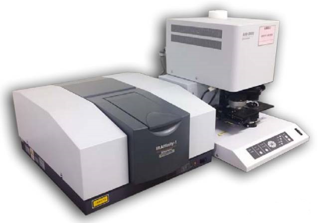
In PCB/PCBA failure analysis, it combines the attenuated total reflection (ATR) with infrared microscopy (AIM). It can have ualitative analysis of organics in pcb manufacturing process and PCB/PCBA surface organic foreign bodies.
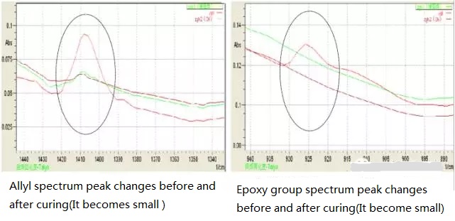
ATR is easy to operate,and it has low requirements on sample preparation.It can detect solid and liquid organic without special treatment .It goes for analysis of large amount of organic of PCB/PCBA,but it is more difficult for small samples for testing.If ATR is used for the analysis of detecting degree of curing solder mask .The solder resist curing involves two processes: photo curing and heat curing,and they are the chemical reaction of propenyl group and an epoxy group in the ink ,respectively. FTIR Infrared spectra can detect the changes of functional groups before and after curing in ink ,to determine the curing situation of the solder resist.
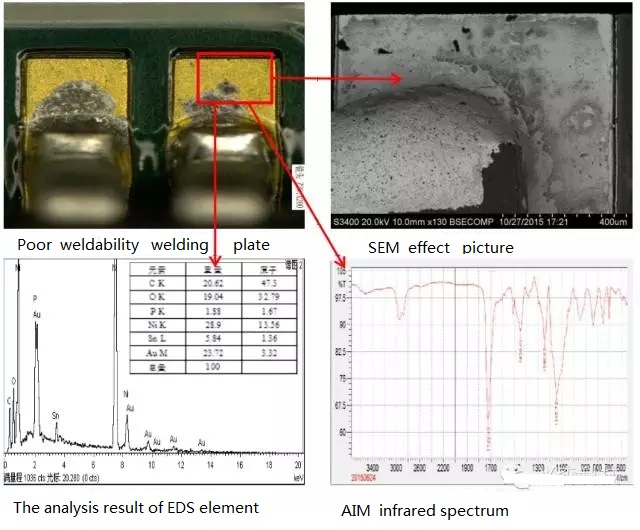
AIM compensate for the inadequacies of the ATR. For small sample, it has excellent detection performance,and it can detect the sample with the square less than 10μm * 10μm.At the same time, the amount of sample is required less.In theory, it can detect micron-level trace samples.In PCB \ PCBA failure analysis ,we usually use EDS to do compositional analysis of small amounts of substances,but EDS mainly analyze element content,and can not do the analysis for H.The analysis of organic is helpless.AIM ,as trace organics detection means,solve the problem of analyzing the pad surface trace organic. In the actual failure analysis,the joint use between AIM and EDS can do a comprehensive analysis of material composition.
The infrared thermal imager
Infrared Thermal Camera is widely used to observe the surface temperature distribution.It can test the temperature distribution of objects under different conditions.Temperature monitoring range can reach 0-250 ℃,which has a wide range of testing.The sensitivity of testing the temperature is better than 100mK,which can clearly react the temperature distribution of the surface of the object in different regions.
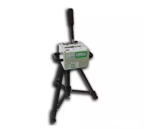
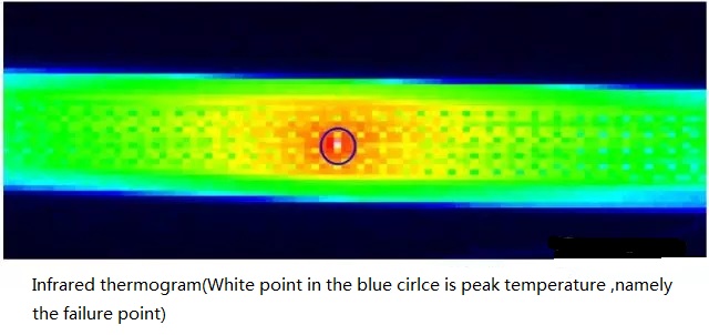
Infrared thermal camera use measured target’s infrared radiation energy distribution graphics,which are received by infrared detectors and optical imaging lens ,to reflect on the photosensitive element of infrared detectors,and thereby get the infrared thermography.This thermography is corresponds to the heat distribution field of the surface of objects.The different colours in the thermography represent different temperature of tested objects. Usually white is set to maximum temperature.
In PCB / PCBA failure analysis applications,infrared imaging ,as a means of non-destructive analysis, can locate complex networks ajar failpoints .The external current is applied to the PCB/PCBA failure network. Infrared camera observe the temperature distribution of PCB / PCBA surface.The failpoints will present the highest temperature point on the PCB/PCBA infrared thermogram,which can quickly locate ajar failpoints in complex network. This approach greatly improves the efficiency and accuracy of the failure analysis.
X-Ray Inspection Machine
X-ray is the electromagnetic wave with short wavelength and great energy. Its photon energy is much larger tens of thousands to hundreds of thousands times than visible photon energy, with strong penetration .In physics, industry, agriculture and medicine ,as a means of non-destructive testing,it has been widely used.In the PCB manufacturing and mounting SMT industry,X-Ray detector is a commonly used testing equipment,and its minimum resolution can be up to 250nm,and it can observe the fine features.While its video receiver may have deflection angle of about 70 ° left and right (a total of 140 °) and rotate 360 °, which can achieve muli-directional observation at different angles.
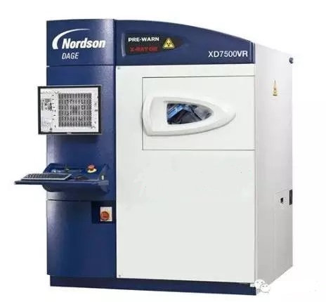
X-ray detection machine generate high-energy X-rays through the X-ray emitting tube,and make the high-energy X-ray irradiate to he test sample surface.Due to different density and atomic weight of sample material itself, the different components have different absorption capacity for the X-rays,and then generate projection on the image receiver.The higher density material has the deeper the shadow,and thus distinguish different material of samples.
In PCB / PCBA failure analysis applications,X-ray, as a means of non-destructive analysis, mainly is used in the analysis of solder joints, cracks, inner short circuit. Solder joints analysis are mainly used in the analysis of soler joints empty thta is generated in the process of SMT, as well as the analysis of cracks and short cut of the PCB circuit.And its analysis can analyze horizontal position and height of the defects by adjusting the viewing angle,and can perform the accurate location.